

Method for preparing high-quality thin film by using ionized atom clusters and combining HIPIMS technology
A high-quality technology of atomic clusters, applied in the direction of ion implantation plating, coating, metal material coating technology, etc., can solve the problems of unstable mechanical properties, poor quality of film materials, and poor film bonding force, etc., to achieve Effects of sputtering yield improvement, bonding force improvement, and HV hardness improvement
- Summary
- Abstract
- Description
- Claims
- Application Information
AI Technical Summary
Problems solved by technology
Method used
Image

Examples
Embodiment 1
[0060] DLC thin film coating process:
[0061] The specific steps are:
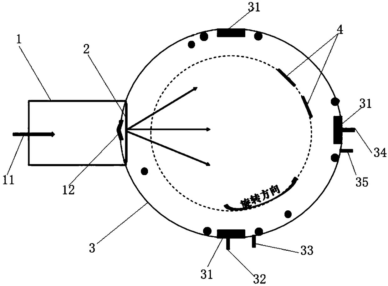
[0062] 1. Introduce one or several inert gases or a mixture of other gases into the cluster generation device to form cluster atoms. The clusters are ionized by the ICP ion source, and the substrate is cleaned by applying 300-500V. The cleaning time is 10min~30min ;
[0063] 2. Using the HIPIMS method, apply a negative bias voltage of 600V~1000V to the substrate, etch the substrate surface for 2min~20min, remove the oxide layer on the substrate surface, and form an activated fresh surface;
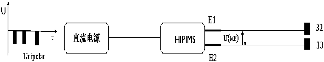
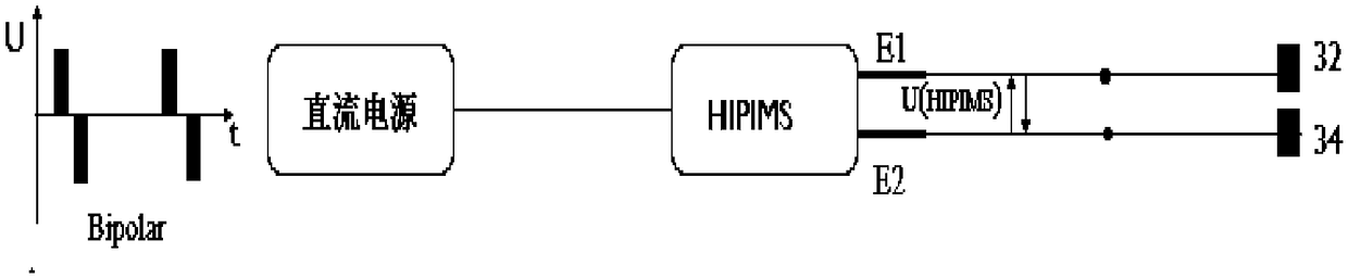
[0064] 3. Adjust the air pressure in the coating chamber to 0.1Pa~1.3Pa, and prepare a transition layer on the substrate. The transition layer is prepared by multi-arc or HIPIMS method to obtain a film layer with excellent bonding force; then use SPIK3000A high-power power supply Sputtering graphite targets with atomic cluster beams of inert gases;
[0065] 4. Coating in a vacuum chamber with a duty cycle of 3%~10%...
Embodiment 2
[0068] SiO2 film preparation process:
[0069] The specific steps are:
[0070] 1. One or several inert gases or a mixture of other gases are introduced into the cluster generation device to form cluster atoms. The clusters are ionized by the ICP ion source, and the substrate is cleaned by applying a bias voltage of 200V-500V. The cleaning time 10min~30min,
[0071] 2. At the same time, use the HIPIMS method to apply a negative bias voltage of 600V~1000V to the substrate, etch the substrate surface for 2min~20min, remove the oxide layer on the substrate surface, and form an activated fresh surface;
[0072] 3. Adjust the air pressure in the coating chamber to 0.1Pa~1.3Pa, and prepare a transition layer on the substrate. The transition layer is prepared by multi-arc or HIPIMS method to obtain a film layer with excellent bonding force; then use SPIK3000A high The power supply uses the atomic cluster beam of inert gas to sputter the graphite target;
[0073] 4. When depositing...
PUM
| Property | Measurement | Unit |
|---|---|---|
| hardness | aaaaa | aaaaa |
Abstract
Description
Claims
Application Information