A method for preparing thin films by transferring sublimable materials from bulk to substrate under non-vacuum conditions

A non-vacuum, bulk technology, used in sustainable manufacturing/processing, semiconductor/solid-state device manufacturing, electrical components, etc. Difficulty and cost problems, achieve the effect of controllable film thickness and solve the difficulty of orthogonal solvent selection

Active Publication Date: 2021-01-19
WUHAN UNIV
View PDF6 Cites 0 Cited by
  • Summary
  • Abstract
  • Description
  • Claims
  • Application Information

AI Technical Summary

Problems solved by technology

[0003] There are two types of existing mature new thin-film photoelectric device preparation technologies: one is based on solution processing through spin coating, scraping coating, inkjet printing and other technologies. This technology has the advantages of high material utilization rate, simple process and low cost. However, there are high requirements for the solubility and film-forming properties of the functional materials used. At the same time, in order to prevent the erosion between the functional layers, the selection of orthogonal solvents is also a major challenge for multilayer solution processable devices; One is to prepare devices based on the high vacuum evaporation process. This technology can avoid the selection of orthogonal solvents, and facilitate the adjustment of various functional materials to adapt to the energy level, so as to obtain better device performance. However, this process requires the molecular weight of the material It cannot be too high and can be sublimated. In addition, the intervention of high vacuum equipment further increases the difficulty and cost of device preparation

Method used


Image

  • A method for preparing thin films by transferring sublimable materials from bulk to substrate under non-vacuum conditions
  • A method for preparing thin films by transferring sublimable materials from bulk to substrate under non-vacuum conditions
  • A method for preparing thin films by transferring sublimable materials from bulk to substrate under non-vacuum conditions

Examples


Embodiment 1

[0036] Fabrication of Upright Organic Electroluminescent Devices Containing Monolayer Transferred Light-Emitting Layers

[0037] Monolayer film transfer at atmospheric pressure

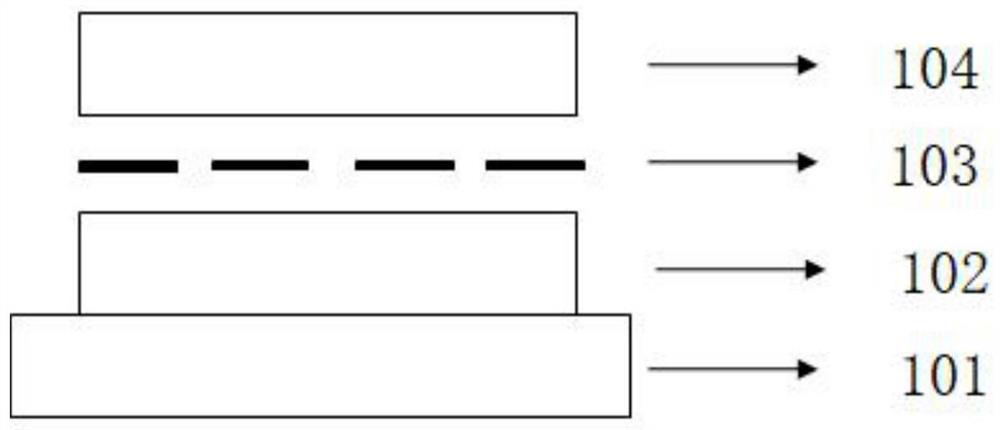
[0038] In this example, the organic thin film is prepared by the heating transfer method under normal pressure, and the schematic diagram of the technical process is as follows figure 1 As shown, in the specific method, the glass substrate (101) and the ITO glass (104) without a receiving medium are first subjected to ultraviolet ozone treatment for 20 minutes, and the specific process can refer to methods known in the art, such as references (J.Phys. Chem. Lett. 2018, 9, 1547-1553). First spin the conductive polymer-poly(3,4-ethylenedioxythiophene)-polystyrenesulfonic acid (PEDOT:PSS) on the ITO glass and bake it at 120°C for 10 minutes, then spin it with chlorobenzene solution Apply a layer of conductive polymer polyvinylcarbazole (PVK) and bake at 120°C for 10 minutes; then, drop 9,9-dimethyl-10-...

Embodiment 2

[0043] Light-emitting preparation of positive organic electroluminescent devices containing double-layer transfer materials;

[0044] Bilayer film transfer at atmospheric pressure

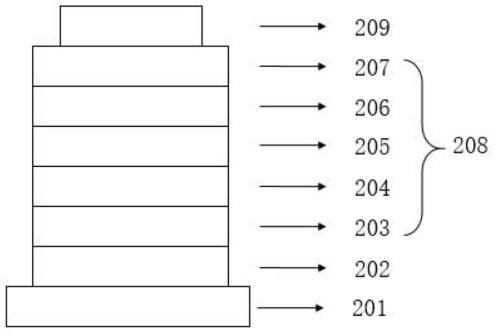
[0045] In this embodiment, the thin film is prepared by the normal pressure heating transfer method. The specific method is to first conduct the ultraviolet ozone treatment on the conductive glass (ITO) substrate and the ordinary glass substrate for 20 minutes. The specific process can refer to methods known in the art, such as references ( J. Phys. Chem. Lett. 2018, 9, 1547-1553). First spin PEDOT:PSS on the ITO glass and bake it at 120°C for 10 minutes, then spin-coat a layer of dendritic compound 10,10'-(sulfonyl(4,1-phenylene) with chlorobenzene solution )) bis(2,7-bis(3,6-di-tert-butyl-9H-carbazol-9-yl)-9,9-dimethyl-9,10-dihydroacridine (4CzDMAC- DPS); Then, drip the 1:1 mixed solution of chlorobenzene and chloroform of DPEPO on the glass sheet that ultraviolet ozone is processed, spin 30 se...

Embodiment 3

[0050] Fabrication of Perovskite Electroluminescent Devices Containing a Monolayer Transferred Electron Transport Layer

[0051] Monolayer film transfer at atmospheric pressure

[0052] In this embodiment, the thin film is prepared by the normal pressure heating transfer method. The specific method is to first conduct the ultraviolet ozone treatment on the conductive glass (ITO) substrate and the ordinary glass substrate for 20 minutes. The specific process can refer to methods known in the art, such as references ( J. Phys. Chem. Lett. 2018, 9, 1547-1553). First spin PEDOT:PSS on the ITO glass and bake it at 120°C for 10 minutes, then spin coat a layer of methylamine bromide with a mixed solution of dimethylsulfoxide (DMSO) and dimethylformamide (DMF) Lead (MAPbBr 3 ), the solution preparation process can refer to methods known in the art, such as references (ACS Nano, 2017, 11, 3311-3319); then, drop 4,7 on another glass substrate that has been cleaned and treated with ult...


PUM

PropertyMeasurementUnit
thicknessaaaaaaaaaa
thicknessaaaaaaaaaa
thicknessaaaaaaaaaa

Abstract

The invention relates to a method for preparing a thin film by transferring a sublimable material from a body to a substrate under non-vacuum conditions. The molecular weight of the sublimable material is less than or equal to 1000 g / mol. The preparation method includes the following steps: preparing the sublimable material on the surface of the body Film or make a sheet, and then align the side of the body containing the above-mentioned sublimable material with the side of the substrate that needs to be filmed, and heat the side of the body that is not in contact with the sublimable material under non-vacuum conditions to ensure the transfer of the sublimable material. To the substrate, a thin film is prepared on the surface of the substrate material. The method of the invention can prepare single-layer or continuous multi-layer films under non-vacuum conditions, and the film thickness is controllable, which solves the difficulty of selecting orthogonal solvents in the process of using solution processing methods in the preparation of multi-layer thin film devices in the prior art problems and the high cost of vacuum evaporation.

Description

technical field [0001] The invention belongs to the technical field of film material preparation, and in particular relates to a method for transferring a sublimable material from a carrier to a substrate to form a film under non-vacuum conditions. Background technique [0002] New thin-film optoelectronic devices, such as organic electroluminescence (OLED), organic photovoltaic devices (OPV), quantum dot light-emitting devices, quantum dot photovoltaic devices, perovskite light-emitting devices and perovskite photovoltaic devices, are research hotspots, promoting technological innovation and technological change. Different from the traditional inorganic optoelectronic devices relying on the long single crystal process, the preparation process of this new type of optoelectronic devices is relatively simple, the material modification is flexible and changeable, and it can meet the needs of industrialization such as large area and low cost. [0003] There are two types of exi...

Claims


Application Information

Patent Timeline
Patent Type & Authority Patents(China)
IPC IPC(8): H01L51/48H01L51/56H01L51/42H01L51/50
CPCH10K71/16H10K30/20H10K30/30H10K50/11Y02E10/549Y02P70/50
Inventor 谢国华杨楚罗相烨鹏
Owner WUHAN UNIV
Why Eureka
Try Eureka