Supercharge Your Innovation With Domain-Expert AI Agents!

Semiconductor device structure and formation method

A device structure and semiconductor technology, applied in semiconductor devices, semiconductor/solid-state device manufacturing, electric solid-state devices, etc., can solve problems such as MOS tube output curve abnormality, device performance degradation, and effective connection formation, so as to avoid self-heating effect, Increased switching speed and reduced contact resistance

Active Publication Date: 2019-04-12
上海微阱电子科技有限公司
View PDF3 Cites 0 Cited by
  • Summary
  • Abstract
  • Description
  • Claims
  • Application Information

AI Technical Summary

Problems solved by technology

But since the device is fully isolated, figure 1 The body region 14 of the NMOS and PMOS in the system cannot be effectively connected to the power supply or ground, forming the so-called floating body effect
Although the floating body effect can be improved through the device layout, due to the large resistance of the body region 14, when the body contact region is far away from the channel region, the floating body effect will still appear, resulting in an abnormal output curve of the MOS transistor
At the same time, the thermal conductivity of the silicon dioxide 12 below the body region 14 is poor, which causes the self-heating effect of the device, reduces the carrier mobility of the device, and degrades the performance of the device.
In addition, the preparation process of SOI silicon wafer is complicated and the manufacturing cost is high

Method used


Image

  • Semiconductor device structure and formation method
  • Semiconductor device structure and formation method
  • Semiconductor device structure and formation method

Examples


Embodiment Construction

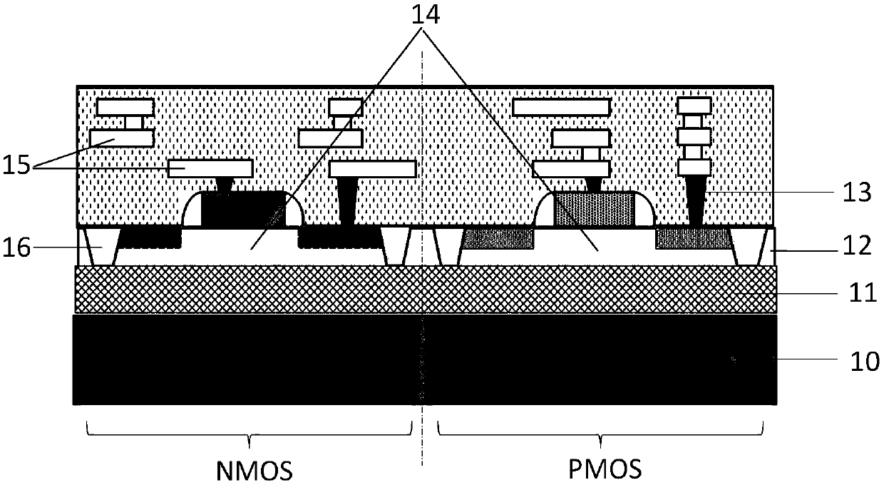
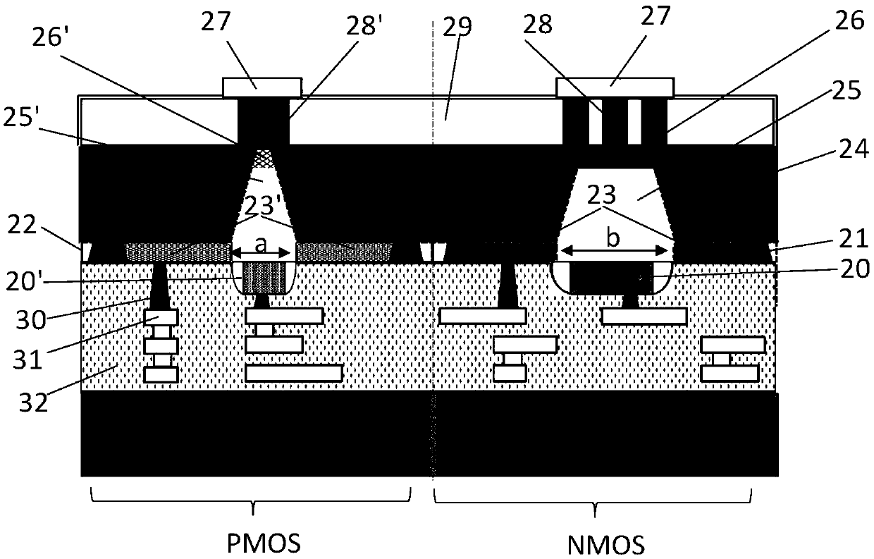
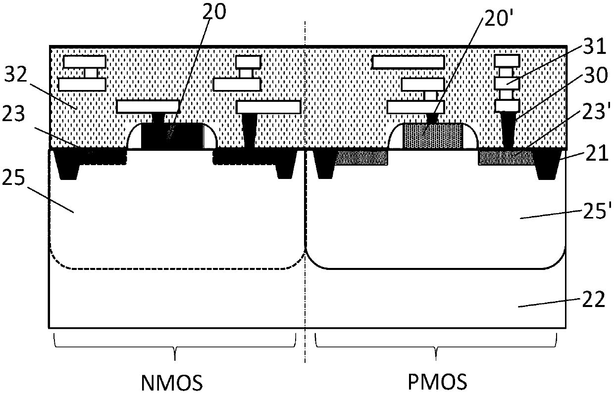
[0042] The specific embodiment of the present invention will be further described in detail below in conjunction with the accompanying drawings.

[0043] It should be noted that, in the following specific embodiments, when describing the embodiments of the present invention in detail, in order to clearly show the structure of the present invention for the convenience of description, the structures in the drawings are not drawn according to the general scale, and are drawn Partial magnification, deformation and simplification are included, therefore, it should be avoided to be interpreted as a limitation of the present invention.

[0044] In the following specific embodiments of the present invention, please refer to figure 2 , figure 2 It is a schematic diagram of a semiconductor device structure in a preferred embodiment of the present invention. Such as figure 2 As shown, a semiconductor device structure of the present invention includes multiple structures disposed on...


PUM


Abstract

The invention discloses a semiconductor device structure. A conventional semiconductor substrate is used for manufacturing a device, and complete dielectric isolation between devices is realized by virtue of connection between back surface trench isolation and shallow trench isolation; the bottom of the back surface trench isolation is in contact with N+ source drain and P+ source drain, so that parasitic capacitance between N+ source drain and a P well, and between the P+ source drain and an N well is eliminated, and the switching speed of an MOS device is increased; through processes of backsurface N+ injection and P+ injection, a back surface contact hole and a back surface metal layer, the P well of an NMOS is grounded, the N well of a PMOS is connected with the power supply, and theseries resistance of the body contact is reduced, so that the floating body effect of an SOI device is avoided; and in addition, the back surface contact hole is connected with the side walls of an N-well active region and a P-well active region on a silicon substrate, so that the heat generated in the device can be rapidly guided out through the contact holes and the metal layer, the self-heatingeffect is avoided, and the performance degradation of the device is prevented. The invention further discloses a formation method of the semiconductor device structure.

Description

technical field [0001] The present invention relates to the technical field of semiconductor processing, and more particularly, to a structure and a forming method of a semiconductor device. Background technique [0002] For half a century, the semiconductor industry has followed Moore's Law to shrink transistor size, increase transistor density, and improve performance step by step. However, as the size of bulk silicon transistor devices with planar structure is getting closer to the physical limit, Moore's law is getting closer to its end; therefore, some new structures of semiconductor devices called "non-classical CMOS" have been proposed. These technologies include FinFET, carbon nanotubes and silicon on insulator (silicon on insulator, SOI), silicon germanium on insulator (SiGe on insulator: SiGeOI) and germanium on insulator (Ge on insulator: GeOI), etc. Through these new structures, the performance of semiconductor devices can be further improved. [0003] Among th...

Claims


Application Information

Patent Timeline
IPC IPC(8): H01L27/092H01L21/8238
CPCH01L27/0922H01L21/8238H01L21/823814H01L21/823878
Inventor 顾学强
Owner 上海微阱电子科技有限公司
Features
  • R&D
  • Intellectual Property
  • Life Sciences
  • Materials
  • Tech Scout
  • Unparalleled Data Quality
  • Higher Quality Content
  • 60% Fewer Hallucinations
Learn More