Preparation method of organic small molecule crystal patterned array

A technology of crystal patterns and small molecules, which is applied in the manufacture of semiconductor/solid-state devices, electric solid-state devices, semiconductor devices, etc., can solve the problems of complicated etching steps, high price, human body damage by fluorinated etching plasma, etc., and achieve the growth method Simple, easy to design, low cost effect

Inactive Publication Date: 2019-04-30
BEIJING SCITECH NANOTECH CO LTD
View PDF3 Cites 8 Cited by
  • Summary
  • Abstract
  • Description
  • Claims
  • Application Information

AI Technical Summary

Problems solved by technology

However, the preparation of silicon pillar templates requires complicated etching steps, and the price is high (2000RMB / 4inch Si wafer), and its fluorinated etching plasma (CF 4 ) is very harmful to the human body

Method used


Image

  • Preparation method of organic small molecule crystal patterned array
  • Preparation method of organic small molecule crystal patterned array
  • Preparation method of organic small molecule crystal patterned array

Examples


Embodiment 1

[0059] Carry out the preparation method of photoresist template as described in technical scheme 1.1:

[0060] 1.1 Preparation of photoresist template:

[0061] 1.1.1 Spin coating: Spin a layer of SU-8 2015 photoresist on a clean silicon wafer (cleaned by standard RCA method) with a homogenizer, the speed of the homogenizer is 7000rpm, and the thickness of the photoresist layer is 6μm;

[0062] 1.1.2 Pre-baking: Carry out pre-baking treatment on the glue baking machine, so that the photoresist is thermally cured, the baking temperature is 95 ° C, and the baking time is 2 minutes;

[0063] 1.1.3 UV exposure: Use a UV lithography machine to expose the photoresist film through the mask and control the exposure dose. The exposure dose is 100mJ / cm 2 ;

[0064] 1.1.4 Post-baking: Carry out post-baking treatment on the glue baking machine to form the patterned structure. The baking temperature is 95°C and the baking time is 3.5 minutes;

[0065] 1.1.5 Developing: use the photoresi...

Embodiment 2

[0070] Carry out patterned growth of organic small molecule crystals according to the method described in technical scheme 1.2:

[0071] 1.2 Patterned growth of small organic molecule crystals:

[0072] 1.2.1 Prepare a toluene solution of TIPS-pentacene with a concentration of 1.5 mg / ml;

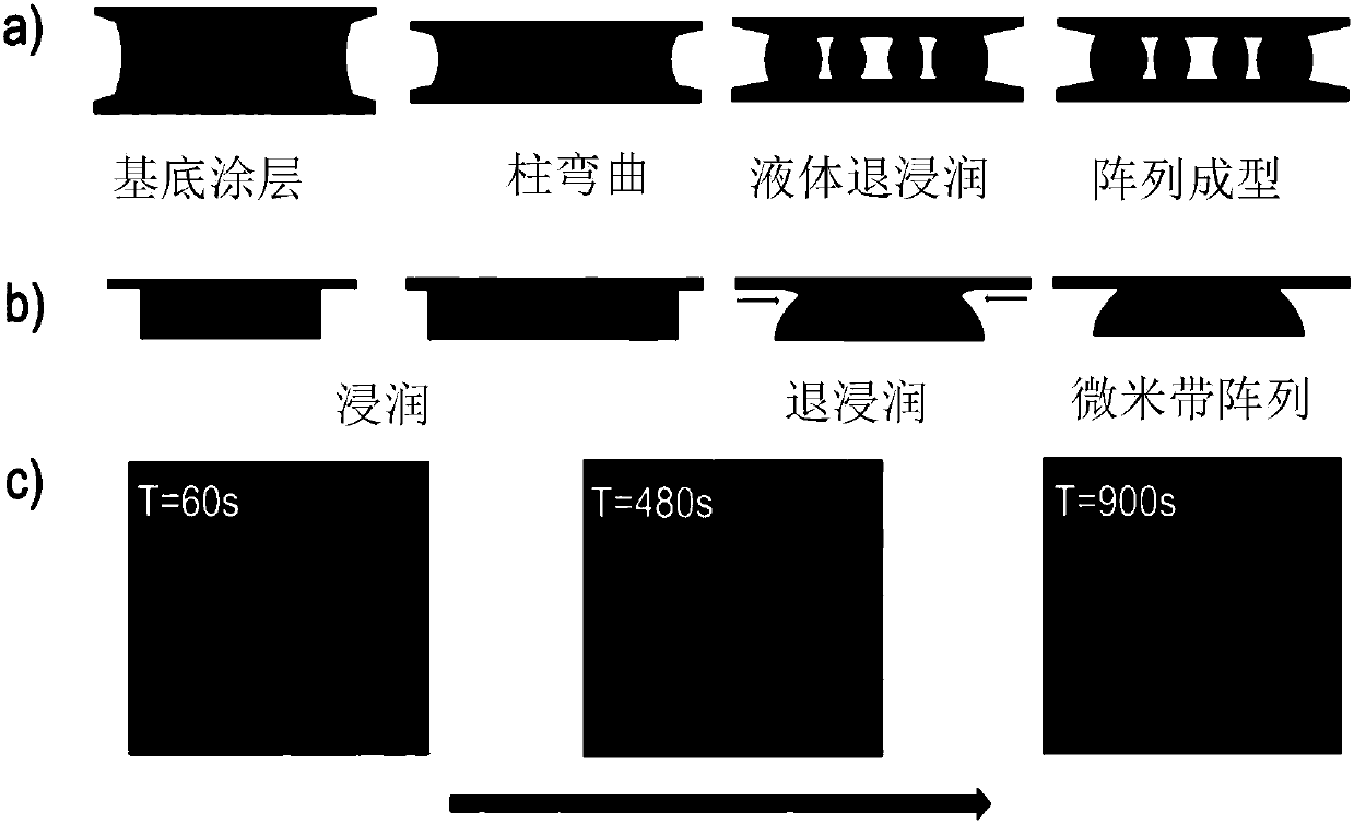
[0073] 1.2.2 Capillary force printing method of "sandwich" structure system: 5 μl of solution is added dropwise on the photoresist template prepared in Example 1, and the OTS (octadecyltrichlorosilane) modified silica substrate Cover the top of the photoresist template and fix it with a long tail clip to form a sandwich structure. Under the joint action of template induction and capillary force, a TIPS-pentacene crystal patterned structure can be directly generated on the target substrate.

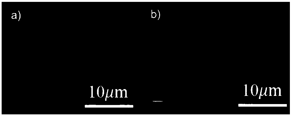
[0074] Experimental results: if image 3 Shown is the growth schematic diagram of the "sandwich" system and the actual fluorescence monitoring image. It can be found that under the induction of the pho...

Embodiment 3

[0076] On the basis of Example 2, by adjusting the concentration of the solution, a size-adjustable pentacene (TIPS-pentacene) microribbon array can be obtained.

[0077] 1.2 Patterned growth of small organic molecule crystals:

[0078] 1.2.1 Prepare a toluene solution of TIPS-pentacene with a concentration of 0.3-1.5mg / ml;

[0079] 1.2.2 Capillary force printing method of "sandwich" structure system: 5 μl of solution is added dropwise on the photoresist template prepared in Example 1, and the OTS (octadecyltrichlorosilane) modified silica substrate Cover the top of the photoresist template and fix it with a long tail clip to form a sandwich structure. Under the joint action of template induction and capillary force, a TIPS-pentacene crystal patterned structure can be directly generated on the target substrate.

[0080] Experimental results: if Figure 5 As shown, by adjusting the growth concentration of the reaction solution, a size-adjustable microribbon array can be obtai...


PUM


Abstract

The invention discloses a preparation method of an organic small molecule crystal patterned array. The preparation method includes the following steps: 1) preparing a photoresist-based elastic patterned template by ultraviolet photolithography; and 2) preparing an aqueous solution or organic solution of organic small molecules by taking the photoresist-based elastic patterned template as an induction template and taking a target substrate as a cover plate, and preparing the organic small molecule crystal patterned array by using a capillary printing method based on a sandwich structure system.The preparation method of the organic small molecule crystal patterned array uses the capillary printing method, which is easy in implementation, chip and efficient, of inducing the growth of the organic small molecule crystal patterned array by the template to facilitate applications of devices.

Description

technical field [0001] The invention belongs to the field of crystal growth, micro-processing and microelectronic devices, in particular, the invention relates to a method for preparing a patterned array of organic small molecule crystals. Background technique [0002] Due to the designability of its molecular structure and the orderliness of molecular arrangement during its assembly, organic semiconductor single crystal materials have a wide range of applications in optoelectronic fields such as sensors, light-emitting diodes, photodetectors, and photovoltaic devices. Among them, organic small molecule crystals are widely used in the field of organic field effect transistors due to their good crystallinity and low defect density. Organic field effect transistors with high mobility are good substitutes for silicon-based field effect transistors. [0003] The preparation of small molecular crystals by the liquid phase method has relatively loose requirements on instruments an...

Claims


Application Information

Patent Timeline
Patent Type & Authority Applications(China)
IPC IPC(8): H01L51/00H01L51/05H01L51/40
CPCH10K71/13H10K71/233H10K10/462H10K99/00H10K10/00
Inventor 吴雨辰高寒飞江雷
Owner BEIJING SCITECH NANOTECH CO LTD
Why Eureka
Try Eureka