Boron doped diamond electrode and preparation method thereof
A diamond electrode, boron doping technology, applied in chemical instruments and methods, metal material coating process, ion implantation plating, etc. The problem of unstable titanium oxide passivation layer, etc., can achieve the effect of inhibiting the formation of loose carbide layer, excellent film-base bonding performance, and good electrochemical catalytic performance.
- Summary
- Abstract
- Description
- Claims
- Application Information
AI Technical Summary
Problems solved by technology
Method used
Image
Examples
Embodiment 1
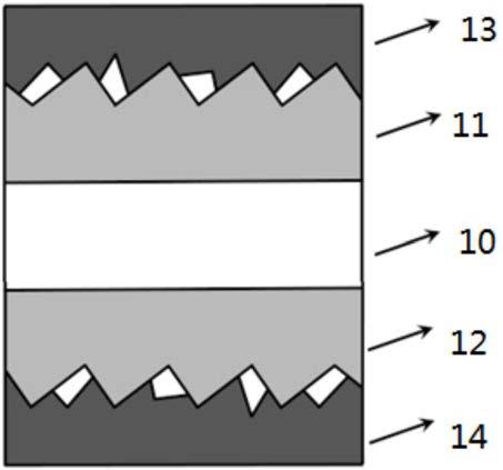
[0046] A method for preparing a boron-doped diamond electrode, comprising the steps of:
[0047] (1) Substrate pretreatment:
[0048] Take the titanium substrate, first sandblast the titanium substrate, then ultrasonically clean the titanium substrate in acetone and alcohol for 15 minutes, and dry it for later use;
[0049] (2) Preparation of TiB by deposition 2 Transition layer and Ti metal layer:
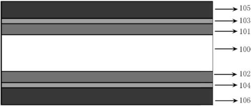
[0050] Using titanium diboride as the target material, a titanium diboride transition layer with a thickness of 300nm was prepared on both sides of the titanium substrate by magnetron sputtering. The magnetron sputtering deposition conditions were: deposition temperature 300°C, argon The gas flow rate is 200sccm, the total reaction pressure is 0.8-1.0Pa, the target negative bias is 100V, the current is 25A, the target power is 2.4KW; the distance between the target and the sample is 70 cm, and the deposition time is 1 hour. The sample is continuously rotated during preparation....
Embodiment 2
[0057] A method for preparing a boron-doped diamond electrode, comprising the steps of:
[0058] (1) Substrate pretreatment:
[0059] Take the titanium substrate, first sandblast the titanium substrate, then ultrasonically clean the titanium substrate in acetone and alcohol for 15 minutes, and dry it for later use;
[0060] (2) Preparation of TiB by deposition 2 Transition layer and Ti metal layer:
[0061] Using titanium diboride as the target material, a titanium diboride transition layer with a thickness of 100nm was prepared on the side of the titanium substrate by magnetron sputtering. The magnetron sputtering deposition conditions were: deposition temperature 300°C, argon gas The flow rate is 200sccm, the total reaction pressure is 0.8-1.0Pa, the target negative bias is 100V, the current is 25A, the target power is 2.4KW; the distance between the target and the sample is 70 cm, and the deposition time is 20 minutes. The sample rotates continuously during the process. ...
Embodiment 3
[0065] A method for preparing a boron-doped diamond electrode, comprising the steps of:
[0066] (1) Substrate pretreatment:
[0067] Take the titanium substrate, first sandblast the titanium substrate, then ultrasonically clean the titanium substrate in acetone and alcohol for 15 minutes, and dry it for later use;
[0068] (2) Preparation of TiB by deposition 2 Transition layer and Ti metal layer:
[0069] Using titanium diboride as the target material, titanium diboride transition layers with a thickness of 300nm were prepared on both sides of the titanium substrate by magnetron sputtering. The magnetron sputtering deposition conditions were: deposition temperature 300°C, The flow rate of argon is 200sccm, the total reaction pressure is 0.8-1.0Pa, the target negative bias is 100V, the current is 25A, the target power is 2.4KW; the distance between the target and the sample is 70 cm, and the deposition time is 1 hour , the sample is continuously rotated during preparation....
PUM
| Property | Measurement | Unit |
|---|---|---|
| thickness | aaaaa | aaaaa |
| thickness | aaaaa | aaaaa |
| thickness | aaaaa | aaaaa |
Abstract
Description
Claims
Application Information


