Preparation method of AlGaN-based 3D flip-chip MSM array ultraviolet detector
A UV detector and flip-chip technology, which is applied in semiconductor devices, final product manufacturing, sustainable manufacturing/processing, etc. Application, device manufacturing process is complex and other issues, to achieve the effect of mature flip-chip welding technology, help device heat dissipation and current output, and easy implementation
- Summary
- Abstract
- Description
- Claims
- Application Information
AI Technical Summary
Problems solved by technology
Method used
Image
Examples
preparation example Construction
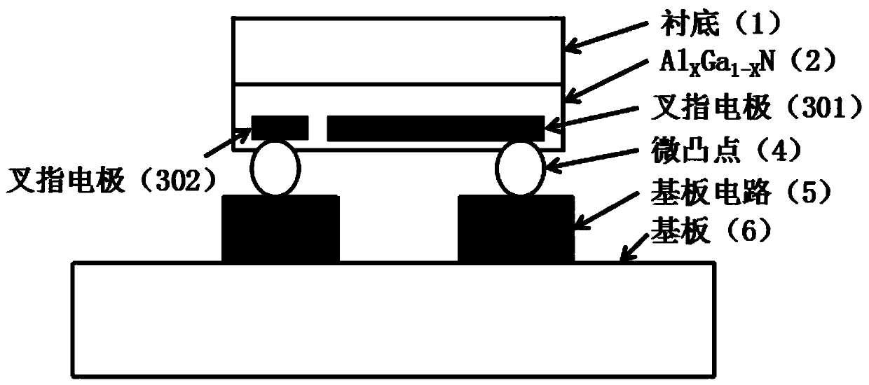
[0036] The invention provides a method for preparing an AlGaN-based 3D flip-chip MSM array ultraviolet detector, comprising the following steps:
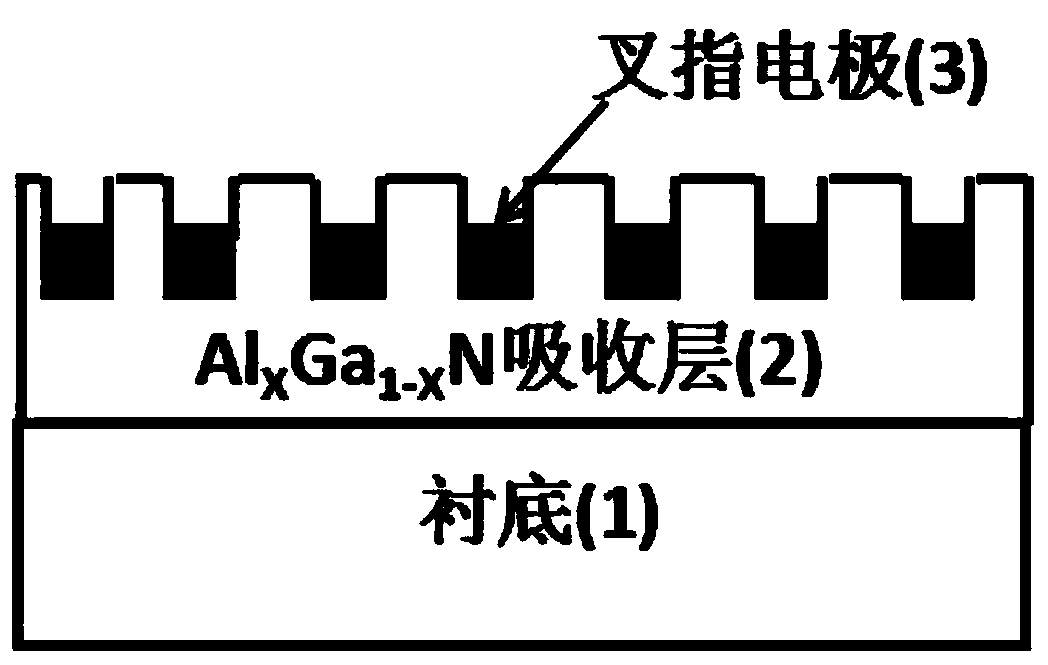
[0037] (1) Epitaxial growth of Al on the substrate 1 X Ga 1-X N ultraviolet light absorbing layer 2;
[0038] (2) in Al X Ga 1-X Perform photolithography on the N ultraviolet light absorbing layer 2, and etch grooves;
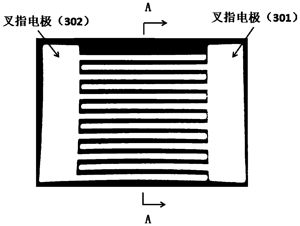
[0039] (3) in Al X Ga 1-X The interdigitated electrode 3 is deposited in the groove of the N ultraviolet light absorbing layer. The interdigitated electrode 3 includes the left interdigitated electrode 301 and the right interdigitated electrode 302. Both ends of the two interdigitated electrodes are provided with large-area pad areas, such as Figure 2-3 As shown, the ultraviolet detector is obtained;
[0040] (4) polishing the back side of the substrate 1;
[0041] (5) On the substrate 6, the substrate circuit 5 is fabricated by using a layout;
[0042] (6) Make soldering micro-bumps 4 on the substrate circ...
Embodiment 1
[0045] The invention provides an AlGaN-based ultraviolet detector and a preparation method thereof, comprising the following steps:
[0046] (1) Choose a plane (0001) plane sapphire with a diameter of 2 inches as the substrate, with a thickness of about 400 μm, and grow Al on the sapphire by MOCVD method 0.32 Ga 0.68 The N ultraviolet absorbing layer has a thickness of about 400nm, in which the Al composition is 0.32, and the forbidden band width of AlGaN with an Al composition of 0.32 corresponds to the wavelength of ultraviolet light to be detected. TMAl and TMGa are respectively used as Al source and Ga source, and silane SiH 4 As a Si source, the Al 0.32 Ga 0.68 Doping of N UV-absorbing layer, Al 0.32 Ga 0.68 The band gap of N corresponds to the wavelength of the ultraviolet light to be detected, which is about 280nm;
[0047] (2) in Al0.32 Ga 0.68 Photolithography is carried out on the surface of the N ultraviolet light absorbing layer, and the interdigitated electr...
PUM
| Property | Measurement | Unit |
|---|---|---|
| Thickness | aaaaa | aaaaa |
| Thickness | aaaaa | aaaaa |
| Thickness | aaaaa | aaaaa |
Abstract
Description
Claims
Application Information
 - R&D
- Intellectual Property
- Life Sciences
- Materials
- Tech Scout
- Unparalleled Data Quality
- Higher Quality Content
- 60% Fewer Hallucinations
Browse by: Latest US Patents, China's latest patents, Technical Efficacy Thesaurus, Application Domain, Technology Topic, Popular Technical Reports.
© 2025 PatSnap. All rights reserved.Legal|Privacy policy|Modern Slavery Act Transparency Statement|Sitemap|About US| Contact US: help@patsnap.com


