Nanocrystalline ink with fluorescence characteristics and preparation method and patterning application thereof

A technology with fluorescent characteristics and nanocrystals, which is applied in the field of nanocrystal inks and its preparation, can solve problems such as poor processing quality, simple device structure, and low efficiency, and achieve the effect of changing

Active Publication Date: 2019-08-06
TSINGHUA UNIV
View PDF10 Cites 8 Cited by
  • Summary
  • Abstract
  • Description
  • Claims
  • Application Information

AI Technical Summary

Problems solved by technology

[0004] However, these research and application works have only solved the problems of the synthesis technology of fluorescent nanomaterials and the application in the field of optoelectronics in a small range.
There are still many excellent properties of fluorescent nanomaterials that have not been fully utilized; the curren

Method used


Image

  • Nanocrystalline ink with fluorescence characteristics and preparation method and patterning application thereof
  • Nanocrystalline ink with fluorescence characteristics and preparation method and patterning application thereof
  • Nanocrystalline ink with fluorescence characteristics and preparation method and patterning application thereof

Examples


Example Embodiment

[0127] Example 1

[0128] This embodiment provides a nanocrystalline ink, which is specifically as follows:

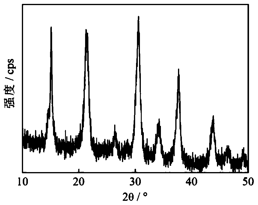
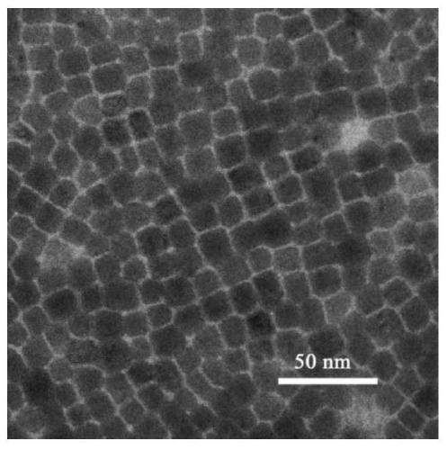
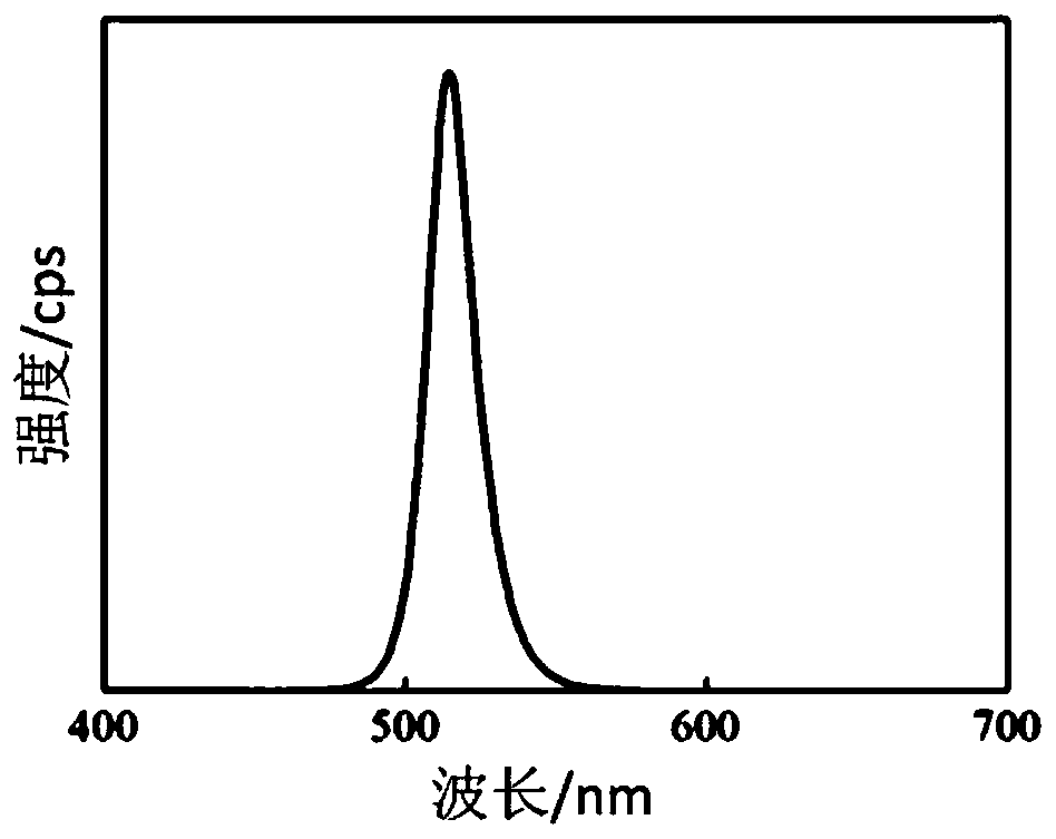
[0129] The nanocrystalline material of this embodiment is CsPbBr 3 Nanocrystal, the XRD pattern of the nanocrystal is as figure 1 As shown, the SEM image of its crystal morphology is as figure 2 As shown, the PL diagram of the fluorescence emission characteristics of the crystal is as image 3 Shown.

[0130]

[0131]

[0132] This embodiment further provides a method for preparing the above-mentioned nanocrystalline ink, as follows:

[0133] According to (n-hexane + n-tetradecane): sodium thiosulfate: CsPbBr 3 Nanocrystalline mass ratio=1:0.0002:0.015 to prepare a mixed solution, and ultrasonically stir for 1h to obtain CsPbI with uniform composition 3 Nanocrystalline dispersion A1;

[0134] Then prepare a mixed solution according to the mass ratio of (n-hexane + n-tetradecane): polyethylene glycol = 1:0.03, and stir for 6 hours under heating at 50°C to obtain a binding soluti...

Example Embodiment

[0140] Example 2

[0141] This embodiment provides a nanocrystalline ink, which is specifically as follows:

[0142] The nanocrystalline material in this embodiment is CsPbBr 3 @CsPbI 3 Nanocrystalline with core-shell structure. CsPbBr used in this example 3 @CsPbI 3 The XRD pattern of the core-shell structured nanocrystal is as follows Figure 4 As shown, the SEM image of its crystal morphology is as Figure 5 As shown, the PL diagram of the fluorescence emission characteristics of the crystal is as Image 6 Shown.

[0143]

[0144] This embodiment further provides a method for preparing the above-mentioned nanocrystalline ink, as follows:

[0145] According to toluene: (sodium dodecylbenzene sulfonate + carboxymethyl cellulose): CsPbBr 3 @CsPbI 3 Nanocrystal mass ratio=1:0.001:0.01 to prepare a mixed solution, and ultrasonically stir for 0.5h to obtain a uniform CsPbBr 3 @CsPbI 3 Nanocrystalline dispersion A2;

[0146] Then, the mixed solution was prepared according to the mass ratio...

Example Embodiment

[0151] Example 3

[0152] This embodiment provides a nanocrystalline ink, which is specifically as follows:

[0153] The nanocrystalline material in this embodiment is CsPbI 3 / rGO nanocomposite heterogeneous crystals. CsPbI used in this example 3 The XRD pattern of / rGO nanocomposite heterogeneous crystal is as follows Figure 7 As shown, the SEM image of its crystal morphology is as Figure 8 As shown, the PL diagram of the fluorescence emission characteristics of the crystal is as Picture 9 Shown.

[0154] Nanocrystalline materialsCsPbI 3 / rGO nanocomposite heterogeneous crystal

[0155] This embodiment further provides a method for preparing the above-mentioned nanocrystalline ink, as follows:

[0156] According to (1,2-dichloroethane + p-xylene): sodium lauryl sulfate: CsPbI 3 / rGO nanocomposite heterogeneous crystal mass ratio=1:0.0002:0.02 to prepare a mixed solution, ultrasonically stir for 3h, and obtain a uniform CsPbI 3 / rGO nanocomposite heterogeneous crystal dispersi...


PUM

PropertyMeasurementUnit
Viscosityaaaaaaaaaa
Viscosityaaaaaaaaaa
Viscosityaaaaaaaaaa

Abstract

The invention relates to nanocrystalline ink with fluorescence characteristics and a preparation method thereof and patterning application thereof. The nanocrystalline ink comprises a nanocrystallinematerial, a dispersant, a binder, a thermal curing agent or a light inducer. The nanocrystal material is selected from one or at least two of an ABX3 nanocrystalline, an ABX3@ABX'3 core-shell structure nanocrystalline composite and a nanocomposite with the ABX3 nanocrystalline grown in situ on the surface of a nano two-dimensional material. The nanocrystalline ink has good fluorescence characteristics, and physical and chemical properties such as ink viscosity meet the basic requirements of inkjet printing. Patterned printing can be realized by inkjet printing. Patterned devices with fluorescence characteristics can be obtained by thermal curing or ultraviolet radiation curing. The nanocrystalline ink can be used in the fields of anti-counterfeiting identification, safety monitoring, intelligent display, building photovoltaic integration, biomedical and visible light wireless communication, and realizes high-quality, large-area, fast and efficient, low-cost and complex-structure deviceprocessing and diversified application.

Description

technical field [0001] The invention relates to the technical field of application of nanomaterials, in particular to a nanocrystalline ink with fluorescent properties, a preparation method thereof, and a patterning application. Background technique [0002] Semiconductor nanocrystals have been widely used in solar cells, light-emitting diodes, photodetection, photocatalysis, lasers and other fields due to their unique photoelectric properties; especially CsPbX 3 (X is a halogen element) is a representative of inorganic perovskite nanocrystals, because of its excellent properties such as high light absorption coefficient, low defect density, long carrier diffusion distance and bipolar carrier transport, it is also favored by researchers. Widespread concern. [0003] The inventor has previously developed a series of in-situ growth CsBX on the surface of nanometer two-dimensional materials 3 (B is an element containing +2 valence state; X is a halogen element) nanocrystallin...

Claims


Application Information

Patent Timeline
IPC IPC(8): C09D11/50C09D11/30B41M5/00B41M3/14B41M3/00G09F13/22G09F3/00H01Q1/24H01Q1/38H01Q1/50
CPCB41M3/00B41M3/14B41M5/00B41M5/0041C09D11/30C09D11/50G09F3/0294G09F13/22G09F2013/225H01Q1/241H01Q1/38H01Q1/50
Inventor 林红张琦石京周养盈魏雅璇
Owner TSINGHUA UNIV
Why Eureka
Try Eureka