Preparation method of gallium-doped silicon ingot, gallium-doped silicon ingot and silicon piece

A technology of silicon ingots and silicon wafers, which is applied in chemical instruments and methods, self-melting liquid pulling method, polycrystalline material growth, etc., can solve the problem of light attenuation rate of polycrystalline gallium-doped silicon wafers, which is not theoretically feasible for chemical reactions fluctuations, resistivity fluctuations of crystalline silicon materials, etc., to achieve the effect of improving photoelectric conversion efficiency, high photoelectric conversion efficiency, and long minority carrier lifetime

Inactive Publication Date: 2019-11-12
HUNAN RED SUN PHOTOELECTRICITY SCI & TECH
View PDF5 Cites 6 Cited by
  • Summary
  • Abstract
  • Description
  • Claims
  • Application Information

AI Technical Summary

Problems solved by technology

However, since the melting point of gallium is about 29.8°C, and its melting point is relatively low, the following problems may occur in the preparation process of gallium-doped crystalline silicon: (1) metal gallium presents a large solid shape during batching, and its weight is difficult to measure, and The measurement accuracy is not high, which affects the resistivity value of crystalline silicon
(2) In the melting process of crystalline silicon preparation, which includes low-temperature vacuum process and high-temperature low-pressure air circulation process, liquid gallium is relatively easy to volatilize, resulting in less gallium actually entering the growth stage, and the resistivity of the prepared crystalline silicon material There are large fluctuations
Although this method discloses the use of gallium-silicon dopant blocks to prepare gallium-doped polycrystalline silicon ingots, it uses gallium oxide and silicon to react to form silicon-gallium alloys, which does not have the theoretical feasibility of chemical reactions, and also introduces high-soluble oxygen, which cannot It is used to prepare doped alloys of crystalline silicon; in this patented technology, during the preparation of crystalline silicon, the gallium-silicon dopant block needs to be partially melted, and its melting amount is not easy to control, resulting in extremely high gallium content in the silicon solution. Large uncertainties, affecting the quality of the prepared crystalline silicon material
[0004] The Chinese patent document with the publication number CN 108315819 A discloses a polycrystalline gallium-doped silicon wafer and its preparation method and a solar cell. The polycrystalline gallium-doped silicon wafer prepared by doping gallium has a relatively low light attenuation ratio, However, the light attenuation rate of polycrystalline gallium-doped silicon wafers fluctuates greatly in this patent, for example, the lowest value of light attenuation ratio is 0.5%, and the highest value is 1.7%. In addition, the process of doping gallium is not carried out in this patent technology optimization, which leads to an uncertainty in the solubility of gallium

Method used


Image

  • Preparation method of gallium-doped silicon ingot, gallium-doped silicon ingot and silicon piece
  • Preparation method of gallium-doped silicon ingot, gallium-doped silicon ingot and silicon piece
  • Preparation method of gallium-doped silicon ingot, gallium-doped silicon ingot and silicon piece

Examples


Embodiment 1

[0029] A preparation method of gallium-doped silicon ingot, comprising the following steps:

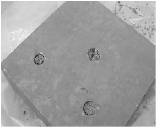
[0030] (1) Use a diamond drill to drill holes in the massive polycrystalline tailings (that is, the silicon material returned to the furnace), and the shape of the holes is cylindrical, and the number is 3, such as figure 1 As shown, wherein the diameter of the circular hole is 10mm and the depth is 30mm. The obtained polycrystalline tailings with holes are cleaned, dried and set aside.

[0031] (2) Use a plastic syringe to inject 4g of liquid metal gallium into the holes of the polycrystalline tailings in step (1), and simultaneously add polycrystalline scraps (being crushed silicon) to the holes to make the crushed silicon and liquid metal The gallium is solidified together to realize the solidification of the liquid gallium metal and the sealing of the circular hole, and obtain the polycrystalline tail material containing the gallium metal, which is the silicon material containing...

Embodiment 2

[0042] A preparation method of gallium-doped silicon ingot, comprising the following steps:

[0043] (1) Get the cylindrical primary polysilicon material (primary silicon material) with bowl-shaped hole, the diameter of its bowl-shaped hole is 40mm, depth is 20mm; With the primary polysilicon material with bowl-shaped hole, clean, dry, spare.

[0044] (2) Use a plastic syringe to inject 2.5g of liquid metal gallium into the bowl-shaped hole of the primary polysilicon material in step (1), and add polycrystalline scrap (silicon scrap) to the bowl-shaped hole at the same time to make the scrap silicon and The liquid metal gallium is solidified together to realize the solidification of the liquid metal gallium and the sealing of the round hole, and obtain the primary polysilicon material filled with metal gallium, that is, the silicon material loaded with metal gallium. The liquid metal gallium used is obtained by melting the metal gallium, specifically: the metal gallium is pla...


PUM

PropertyMeasurementUnit
diameteraaaaaaaaaa
depthaaaaaaaaaa
diameteraaaaaaaaaa

Abstract

The invention discloses a preparation method of a gallium-doped silicon ingot, the gallium-doped silicon ingot and a silicon piece. The preparation method comprises the following steps: injecting a molten metal gallium into pores of a silicon material, curing the molten metal gallium and/or sealing the pores, putting the obtained silicon material with the metal gallium and the rest silicon material into a quartz crucible, and performing melting, recrystallization and annealing cooling so as to obtain gallium-doped silicon ingot. The gallium-doped silicon ingot is prepared by using the preparation method. The silicon piece is prepared from the gallium-doped silicon ingot. By adopting the preparation method, a gallium doping process and effective and precise control on gallium doping amountscan be achieved, the preparation method has the advantages of being convenient in operation, easy in control, high in gallium doping amount precision, and the like, the prepared gallium-doped siliconingot has the advantages of being good in resistance distribution uniformity, long in minority carrier lifetime, and the like, a solar battery prepared from the gallium-doped silicon ingot has high photoelectric efficiency and low light degradation, and great significances can be achieved for wide application of solar batteries.

Description

technical field [0001] The invention belongs to the field of preparation of crystalline silicon materials and semiconductor silicon materials for solar cells, and relates to a preparation method of gallium-doped silicon ingots, gallium-doped silicon ingots and silicon wafers. Background technique [0002] In the field of crystalline silicon material manufacturing, whether it is a single crystalline silicon material or a polycrystalline silicon material, a boron-doped P-type crystalline silicon solar cell will have a light-induced degradation (LID) problem when it is used. With the continuous development of crystalline silicon cell technology, the requirements for its substrate materials are getting higher and higher, and the pursuit of solar cells with higher efficiency and lower light attenuation is the eternal pursuit of the industry. Gallium-doped technology has been proven to significantly reduce the light-induced attenuation of crystalline silicon cells, and has been in...

Claims


Application Information

Patent Timeline
Patent Type & Authority Applications(China)
IPC IPC(8): C30B28/06C30B15/04C30B29/06
CPCC30B15/04C30B28/06C30B29/06
Inventor 明亮黄美玲段金刚刘福刚
Owner HUNAN RED SUN PHOTOELECTRICITY SCI & TECH
Why Eureka
Try Eureka