
High-efficiency light-emitting diode structure and manufacturing method thereof

A light-emitting diode, high-efficiency technology, applied in the field of microelectronics, can solve the problems of reduced luminous efficiency of deep ultraviolet light-emitting diodes, enhanced carrier confinement in quantum wells, reduced ionization rate and hole mobility, etc., to eliminate Quantum-confined Stark effect, increase ionization rate and hole mobility, and increase the effect of barrier height

Inactive Publication Date: 2019-11-29
XIDIAN UNIV
View PDF3 Cites 5 Cited by
  • Summary
  • Abstract
  • Description
  • Claims
  • Application Information

AI Technical Summary

Problems solved by technology

Since the multi-quantum well barrier layer is made of AlGaN material, the Al in the multi-quantum well barrier layer x Ga 1-x N quantum well layer and Al y Ga 1-y There is a difference in the Al composition between the N quantum barrier layers. Through this difference, the electrons and holes of the LED device are confined in the quantum well to generate radiative recombination. However, if the difference is too large, it will cause a significant quantum-confined Stark effect. The difference Too small will cause poor confinement of carriers in the quantum well, so the existing Al x Ga 1-x N / Al y Ga 1-y N multi-quantum well barrier layers cannot enhance the confinement of carriers in quantum wells while weakening the quantum confinement Stark effect
At the same time, the ionization rate and hole mobility of Mg in the p-type layer prepared by AlGaN will decrease with the increase of Al composition, and the decrease of Mg ionization rate and hole mobility will lead to a decrease in the luminous efficiency of deep ultraviolet light-emitting diodes. reduce

Method used


Image

  • High-efficiency light-emitting diode structure and manufacturing method thereof
  • High-efficiency light-emitting diode structure and manufacturing method thereof

Examples


Embodiment 1

[0029] Example 1, preparing a light emitting diode with a light emitting wavelength of 287nm.

[0030] In step one, a bulk gallium nitride substrate is selected and pretreated.

[0031] 1a) Clean the selected substrate: put the substrate into HF acid or HCl acid for ultrasonic cleaning for 5-10 minutes, then put it into acetone solution for ultrasonic cleaning for 5-10 minutes, and then use absolute ethanol solution for ultrasonic cleaning for 5-10 minutes. 10min, then ultrasonic cleaning with deionized water for 5-10min, and finally drying with nitrogen;

[0032] 1b) Place the cleaned substrate in the metal organic chemical vapor deposition MOCVD reaction chamber, and reduce the vacuum degree of the reaction chamber to 3×10 -2 Torr, feed hydrogen gas into the reaction chamber, and under the condition that the pressure of the reaction chamber reaches 25 Torr, heat the substrate to a temperature of 900°C and keep it for 10 minutes to complete the heat treatment of the substrat...

Embodiment 2

[0045] Example 2, preparing a light emitting diode with a light emitting wavelength of 261 nm.

[0046] In step 1, a silicon carbide substrate is selected and pretreated.

[0047] The specific implementation of this step is the same as Step 1 of Example 1.

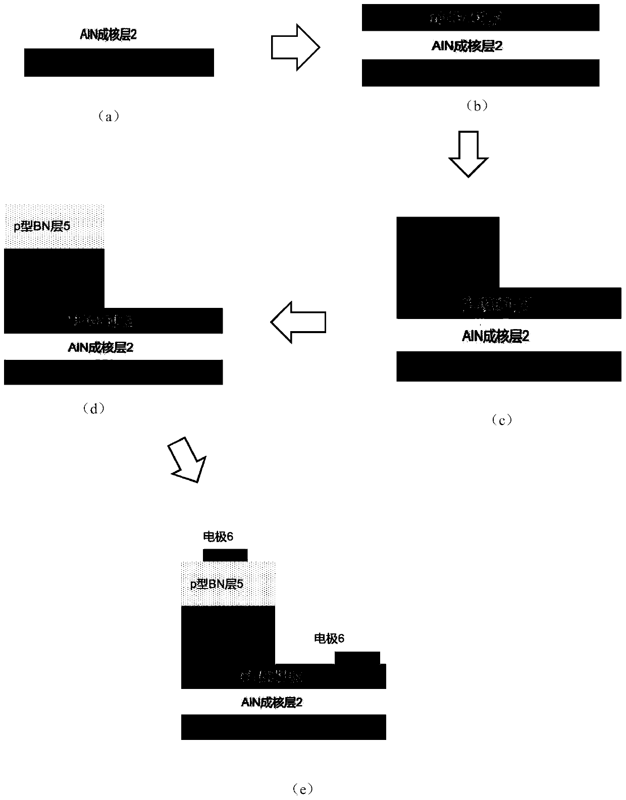
[0048] Step 2, growing a high temperature AlN layer, such as figure 2 (a).

[0049] On the nitrided silicon carbide substrate, the MOCVD process is used under the condition that the temperature of the reaction chamber is 1200°C and the pressure of the MOCVD reaction chamber reaches 340Torr, and the nitrogen source with the flow rate of 3500sccm and the aluminum source with the flow rate of 30sccm are simultaneously introduced to grow A high temperature AlN nucleation layer with a thickness of 30nm.

[0050] Step 3, grow n-type Ga 2 o 3 layer, such as figure 2 (b).

[0051] Under the condition that the temperature of the reaction chamber is 1300°C, an oxygen source with a flow rate of 2700 sccm, a gallium source wi...

Embodiment 3

[0060] Example 3, preparing a light emitting diode with a light emitting wavelength of 233nm.

[0061] In step A, a sapphire substrate is selected and pretreated.

[0062] The specific implementation of this step is the same as step 1 of embodiment 1.

[0063] Step B, using the MOCVD process to grow a high-temperature AlN layer, such as figure 2 (a).

[0064] Set the temperature of the reaction chamber at 1300°C, the pressure of the reaction chamber at 400Torr, and simultaneously feed a nitrogen source with a flow rate of 4000 sccm and an aluminum source with a flow rate of 40 sccm into the reaction, and grow a high-temperature AlN substrate with a thickness of 50 nm on the nitrided sapphire substrate. nuclear layer.

[0065] Step C, using MOCVD process to grow n-type Ga 2 o 3 layer, such as figure 2 (b).

[0066] Raise the temperature of the reaction chamber to 1500°C, reduce the pressure to 60 Torr, and simultaneously feed an oxygen source with a flow rate of 3000 s...


PUM

PropertyMeasurementUnit
Thicknessaaaaaaaaaa
Thicknessaaaaaaaaaa
Thicknessaaaaaaaaaa

Abstract

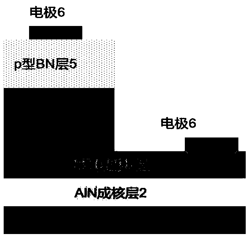
The invention discloses a high-efficiency light-emitting diode structure and a manufacturing method thereof, and mainly solves the problems of low ionization rate and hole mobility of Mg in a p-type region and poor carrier confinement in a quantum well in the prior art. The high-efficiency light-emitting diode structure comprises from bottom to top: a substrate (1), a high-temperature AlN nucleating layer (2) and an n-type Ga2O3 layer (3), wherein an electrode (6) and a working region layer (4) are arranged on the n-type Ga2O3 layer, the working region layer comprises multiple quantum well barrier layers with six periods, each period comprises an AlxGa1-xN quantum well layer and a quantum barrier layer, and a p-type layer (5) and an electrode (6) are arranged on the working region layer. The quantum barrier layer and the p-type layer are prepared from a BN material, so that the quantum confinement stark effect between multiple quantum well barrier layers is eliminated, the ionization rate and the hole mobility of Mg in the p-type layer are improved, the confinement of holes and electrons in quantum wells is enhanced, and the high-efficiency light-emitting diode structure can be used for manufacturing high-efficiency ultraviolet and deep ultraviolet light-emitting equipment.

Description

technical field [0001] The invention belongs to the technical field of microelectronics, and particularly relates to a high-efficiency light-emitting diode, which can be used to manufacture high-efficiency ultraviolet and deep ultraviolet light-emitting devices. [0002] technical background [0003] Since the light-emitting wavelength of AlGaN material can be as short as 200nm, it has become an important material for making ultraviolet and deep ultraviolet light-emitting diodes, and can be widely used in water purification, biological agent detection, sterilization, medicine, etc. [0004] At present, the common ultraviolet light-emitting diodes are grown on the c-plane sapphire substrate, and the structure includes n-type GaN layer, Al x Ga 1-x N / Al y Ga 1-y The N multi-quantum well barrier layer and the p-type layer made of AlGaN realize light emission through the recombination of electrons and holes in the quantum wells. Since the multi-quantum well barrier layer is m...

Claims


Application Information

Patent Timeline
IPC IPC(8): H01L33/06H01L33/32H01L33/00
CPCH01L33/0066H01L33/0075H01L33/06H01L33/32
Inventor 许晟瑞陶鸿昌陈大正朱家铎张雅超李培咸张进成郝跃
Owner XIDIAN UNIV
Learn More