Cross-magnitude multi-scale line width standard and preparation method thereof

A multi-scale, span-scale technology, applied in the direction of instruments, measuring devices, manufacturing tools, etc., can solve the problems of incompatibility with extremely small, poor repeatability, high cost, etc. simple and easy effects

Active Publication Date: 2019-12-03
XI AN JIAOTONG UNIV
View PDF6 Cites 5 Cited by
  • Summary
  • Abstract
  • Description
  • Claims
  • Application Information

AI Technical Summary

Problems solved by technology

[0004] The purpose of the present invention is to provide a cross-scale multi-scale line width standard and its preparation method, which solves the bottleneck that the existing line width standard template cannot be compatible with extremely small (single atomic layer) and extremely large (micron) at the same time In addition, it also solves the defects of high cost, low efficiency or poor repeatability in the preparation process

Method used


Image

  • Cross-magnitude multi-scale line width standard and preparation method thereof
  • Cross-magnitude multi-scale line width standard and preparation method thereof
  • Cross-magnitude multi-scale line width standard and preparation method thereof

Examples


preparation example Construction

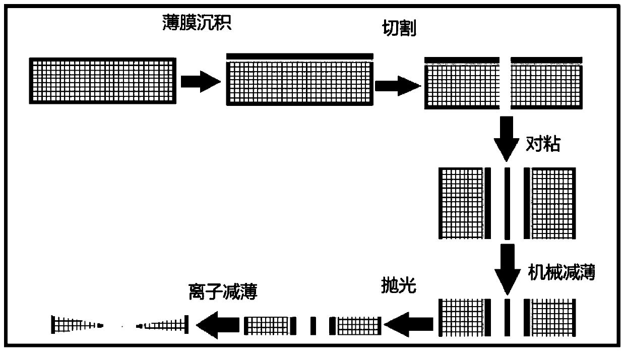
[0031] A method for preparing a span-scale multi-scale linewidth standard provided by the present invention comprises the following steps:

[0032] Step 1, using the atomic layer deposition method to deposit a nano-lamination film formed by two or more materials on the cleaned substrate;

[0033] Among them, the organometallic precursor sources used in the atomic layer deposition method are trimethylaluminum, diethylzinc, tetraethoxysilane, tetrakis(dimethylamino)titanium, tetrakis(methylethylamino)hafnium, tetrakis Any two of (dimethylamino) hafnium, tetrakis (methylethylamino) zirconium and tetrakis (dimethylamino) zirconium.

[0034] The oxygen source used was deionized water (H 2 O), hydrogen peroxide (H 2 o 2 ), oxygen (O 2 ) or ozone (O 3 ).

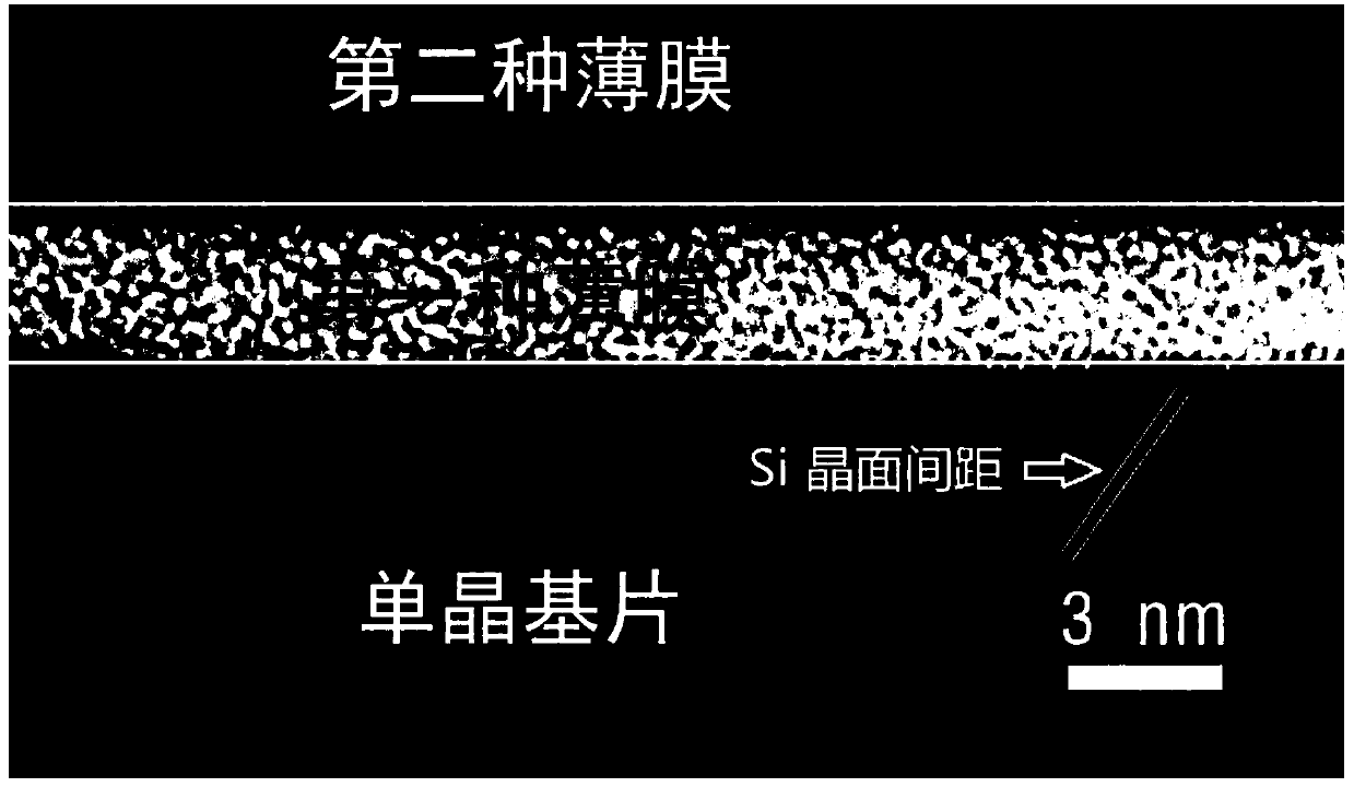
[0035] The deposited first film is SiO 2 film; the deposited second film is a zinc oxide film; the deposited third film is.

[0036] The selected substrate material is an oxide single crystal substrate or a specific orienta...

Embodiment 1

[0047] A method for preparing a span-scale multi-scale linewidth standard provided by the present invention comprises the following steps:

[0048] 1) Cleaning the single crystal Si substrate with RCA standard cleaning process and cleaning its surface with dry nitrogen for subsequent use;

[0049] 2) The single crystal Si substrate processed in step 1 is sent into the atomic layer deposition system through the vacuum loading robot arm of the atomic layer deposition system, and heated to 200°C-300°C to prepare for depositing thin film materials;

[0050] 3) on the basis of step 2, tetraethoxysilane, diethylzinc and deionized water (H 2 O) as precursor sources of Si, Zn and O, respectively, using ALD technology to periodically deposit SiO with a thickness of 3.5 nm on the surface of single crystal Si 2 and 110nm ZnO film; the deposition process parameters are: the first pulse is tetraethoxysilane pulse time is 0.2-0.6, after the pulse is completed, it is purged with 150s ccm ni...

Embodiment 2

[0055] A method for preparing a span-scale multi-scale linewidth standard provided by the present invention comprises the following steps:

[0056] 1) Cleaning the single crystal Si substrate with RCA standard cleaning process and cleaning its surface with dry nitrogen for subsequent use;

[0057] 2) The single crystal Si substrate processed in step 1 is sent into the atomic layer deposition system through the vacuum loading robot arm of the atomic layer deposition system, and heated to 200°C-300°C to prepare for depositing thin film materials;

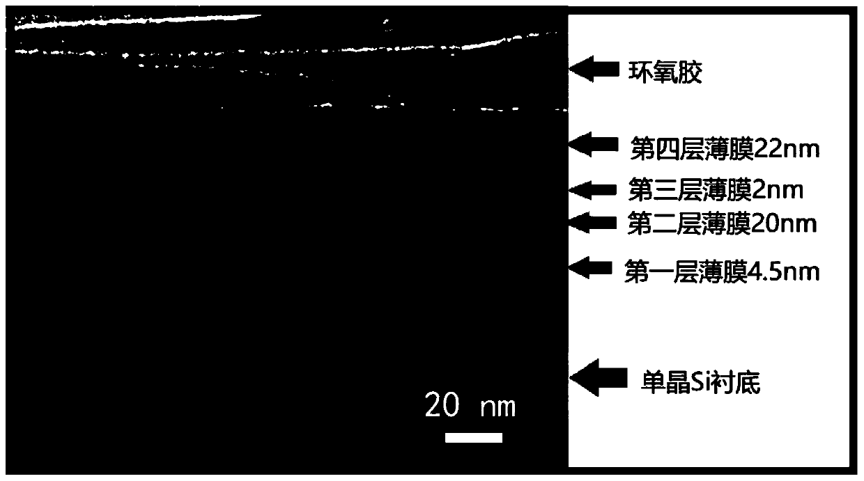
[0058] 3) On the basis of step 2, trimethylaluminum, diethylzinc and deionized water (H 2 O) as precursor sources of Al, Zn and O respectively, using ALD technology to sequentially deposit 4.5nmZnO and 20nmAl on the surface of single crystal Si 2 o 3 , 2nmZnO and 22nm Al 2 o 3 Thin film; the deposition process parameters are: the first pulse is diethyl zinc, and the punching time is 0.1-0.2. After the pulse is completed, it is pur...


PUM

PropertyMeasurementUnit
thicknessaaaaaaaaaa

Abstract

The invention provides a preparation method of a cross-magnitude multi-scale line width standard. The preparation method comprises the following steps: step 1, depositing a nano laminated film formedby two or more than two materials on a clean substrate by utilizing an atomic layer deposition method; step 2, sequentially adhering the nano laminated film obtained in the step 1 to a film surface, heating and curing to obtain a cured sample; step 3, sequentially carrying out mechanical thinning and mechanical polishing on the cured sample obtained in the step 2 to obtain a polished sample; step4, sequentially carrying out ion thinning and ion polishing on the polished sample obtained in the step 3 to finally obtain a cross-magnitude multi-scale line width standard; and the preparation method of the cross-magnitude multi-scale line width standard breaks through the tiny characteristic dimension which cannot be processed by the traditional photoetching + etching technology, can realize the integration of the characteristic dimensions of the line widths with different magnitudes and different scales on the same line width sample plate, and realizes that one line width sample plate meets the requirements of different scales and different fields.

Description

technical field [0001] The invention belongs to the field of nanometrics, and in particular relates to a span-scale multi-scale line width standard and a preparation method thereof. Background technique [0002] So far, the existing line width standard templates usually have only one eigenvalue that can be used as a measurement or the eigenvalues ​​are only in a limited scale, and none of them can collect Angstrom Nanometer (nm) and micron (um) scale multi-scale high-precision linewidth standards. The existing method for making a standard sample of line width can produce a sample of line width ranging from tens of nanometers to several microns. For example: X-ray lithography or synchrotron radiation can produce nanoscale grating linewidth samples, but it needs to use electron synchrotron radiation as a light source, which is very expensive and extremely inconvenient. For ultraviolet lithography, in order to obtain the ultimate resolution, the requirements on the exposure ...

Claims


Application Information

Patent Timeline
Patent Type & Authority Applications(China)
IPC IPC(8): G01B21/04B24B1/00B24B37/04C23C16/455C23C16/56
CPCB24B1/002B24B37/042C23C16/45525C23C16/56G01B21/042
Inventor 张易军王琛英任巍蒋庄德景蔚萱刘明叶作光毛琦
Owner XI AN JIAOTONG UNIV
Why Eureka
Try Eureka