Supercharge Your Innovation With Domain-Expert AI Agents!

Static random access memory

A static random access and memory technology, applied in static memory, digital memory information, information storage, etc., can solve the problems of SRAM operating voltage is difficult to reduce, low integration, high heat generation, etc., to reduce sub-threshold swing, reduce The effect of heat and process structure is simple

Pending Publication Date: 2019-12-03
SHANGHAI HUALI INTEGRATED CIRCUTE MFG CO LTD
View PDF5 Cites 0 Cited by
  • Summary
  • Abstract
  • Description
  • Claims
  • Application Information

AI Technical Summary

Problems solved by technology

[0002] Static random access memory is mainly used as a high-speed cache between the central processing unit (CPU) and the main memory due to its fast speed and the ability to save internal storage data without refreshing the circuit. The shortcomings such as low degree make it mainly used in critical systems to improve efficiency
With the evolution of integrated circuit manufacturing process nodes and the maturity of fin field effect transistor (FinFET) manufacturing technology, the size of FinFET-based SRAM is getting smaller and smaller, but due to the physical limit of the device subthreshold swing (SS) at room temperature is about 60mV / dec, SS indicates the amount of change in gate voltage when the sub-threshold current is changed by 10 times. The physical limit of SS at room temperature makes it difficult to reduce the operating voltage of SRAM, and the problem of high energy consumption needs to be solved urgently

Method used


Image

  • Static random access memory
  • Static random access memory
  • Static random access memory

Examples


Embodiment Construction

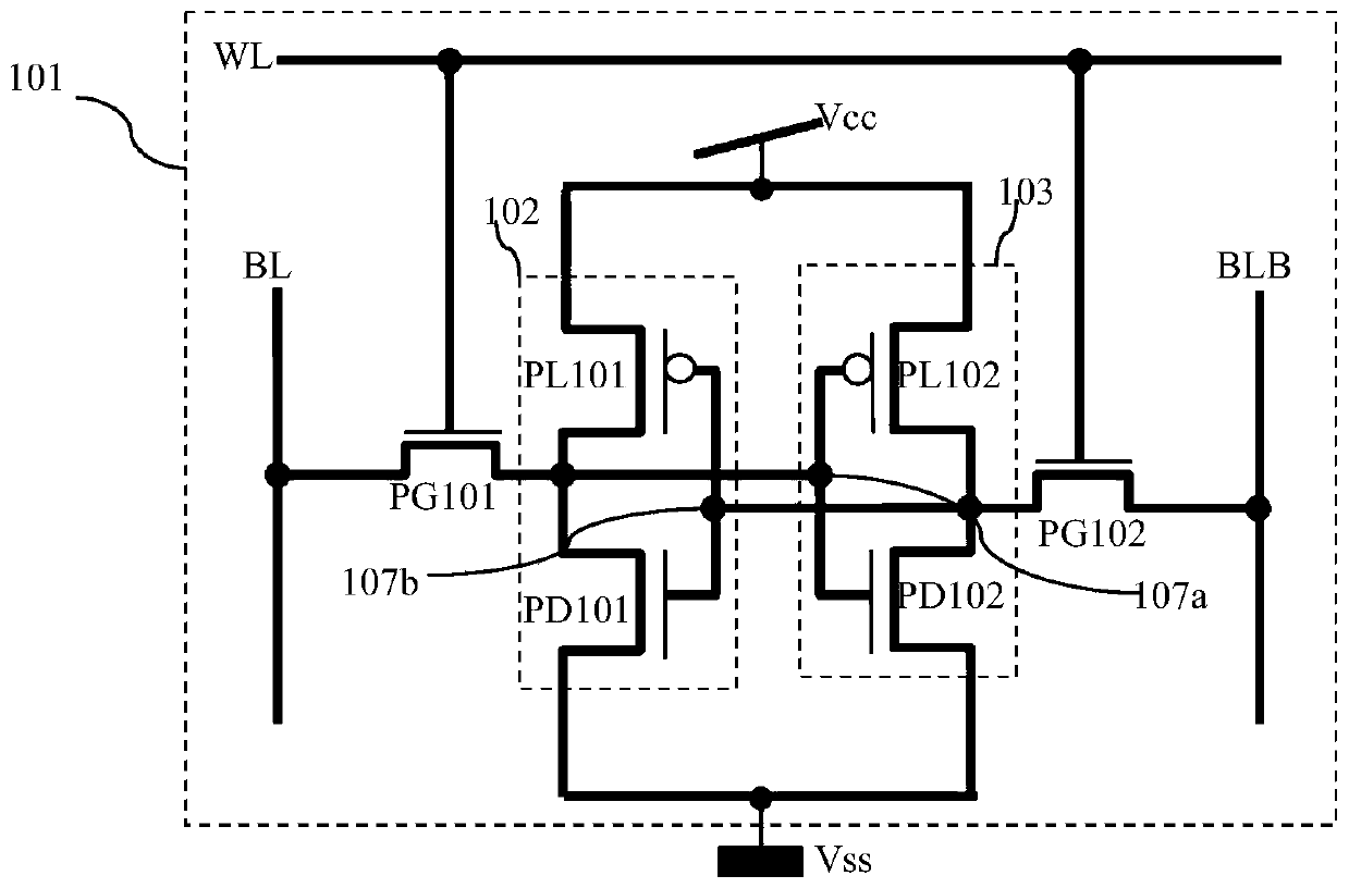
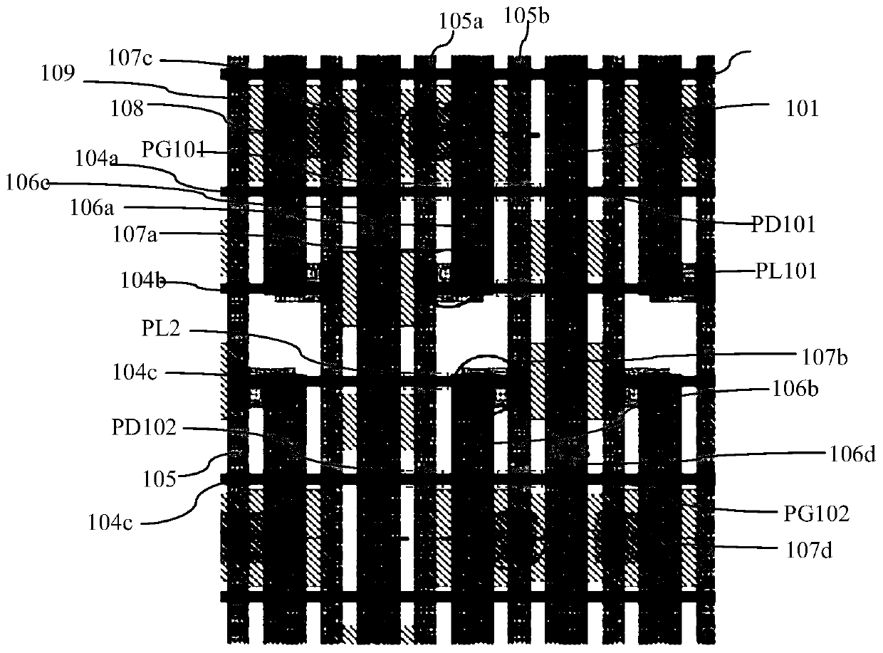
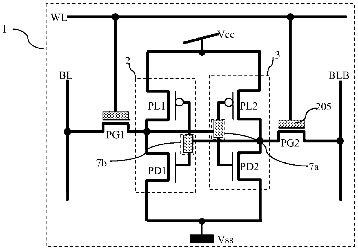
[0079] Such as image 3 Shown is a circuit diagram of the storage unit 1 of the static random access memory of the embodiment of the present invention; Figure 4 Shown is a schematic structural diagram of a fin field effect transistor used in an embodiment of the present invention; Figure 5 What is shown is the layout of the static random access memory of the embodiment of the present invention; the static random access memory of the embodiment of the present invention includes an array structure of a plurality of memory cells arranged in rows and columns.

[0080] Each storage unit 1 includes a first transfer tube PG1, a second transfer tube PG2, a first upper pull tube PL1, a second upper pull tube PL2, a first pull-down tube PD1, and a second pull-down tube PD2; The transmission tube PG1, the second transmission tube PG2, the first pull-down tube PD1, and the second pull-down tube PD2 are all NMOS tubes, and the first pull-up tube PL1 and the second pull-up tube PL2 All are P...


PUM


Abstract

The invention discloses a static random access memory. A storage unit comprises six fin-type field effect transistors. Each fin-type field effect transistor comprises a fin body, a gate structure, a source region and a drain region. The fin body is vertical to an extending direction of the gate structure. The gate structure comprises a gate dielectric layer and a gate conductive material layer. Anegative capacitance material layer is formed on a surface of a gate conductive material layer extending to an external portion of the fin body, a contact hole for leading out the gate conductive material layer is arranged at a top of the negative capacitance material layer, and a gate leading-out electrode formed by a front metal layer interconnection structure is connected through the contact hole at the top of the negative capacitance material layer. The negative capacitance material layer forms a negative capacitor between the gate conductive material layer and the gate leading-out electrode and is connected in series with a dielectric layer capacitor consisting of a semiconductor substrate, a gate dielectric layer and the gate conductive material layer. A sub-threshold swing amplitudeof a transistor of the static random access memory can be reduced so that an operation voltage of the memory can be decreased, and energy consumption and a calorific value are reduced.

Description

Technical field [0001] The present invention relates to a semiconductor integrated circuit, in particular to a static random access memory (SRAM). Background technique [0002] Due to its fast speed, static random access memory can save the internal storage data without refreshing the circuit. It is mainly used as a high-speed cache between the central processing unit (CPU) and the main memory. Shortcomings such as low degree make it mainly used in critical systems to improve efficiency. With the evolution of integrated circuit manufacturing process nodes and the maturity of fin field effect transistor (FinFET) manufacturing technology, the size of FinFET-based SRAM is getting smaller and smaller, but due to the device subthreshold swing (SS) room temperature physical limit is about 60mV / dec, SS represents the amount of change in the gate voltage when the sub-threshold current is changed by 10 times. The room temperature physical limit of SS makes it difficult to reduce the SRA...

Claims


Application Information

Patent Timeline
IPC IPC(8): H01L29/10H01L29/423H01L29/78H01L23/64H01L27/11G11C11/412
CPCH01L29/785H01L29/1033H01L29/42356H01L28/40G11C11/412H10B10/12
Inventor 白文琦李昆鸿王世铭黄志森胡展源
Owner SHANGHAI HUALI INTEGRATED CIRCUTE MFG CO LTD
Features
  • R&D
  • Intellectual Property
  • Life Sciences
  • Materials
  • Tech Scout
  • Unparalleled Data Quality
  • Higher Quality Content
  • 60% Fewer Hallucinations
Learn More