Compound thin film and preparation method thereof, and compound thin film solar cell
A thin-film solar cell and compound technology, applied in circuits, photovoltaic power generation, electrical components, etc., to improve film quality, reduce defects and recombination centers, and promote crystallization
- Summary
- Abstract
- Description
- Claims
- Application Information
AI Technical Summary
Problems solved by technology
Method used
Image
Examples
preparation example Construction
[0039] see figure 1 , an embodiment of the present invention provides a method for preparing a compound thin film, which includes: annealing a Bi-doped absorber layer precursor at a low temperature.
[0040] In detail, in the embodiment of the present invention, through the doping of VA element Bi, during the annealing process, the doped Bi element will react to form a low-melting point compound and act as a flux to promote the crystallization of the absorbing layer film, reducing the film Defects and recombination centers in the film can improve the quality of the film layer, thereby improving the performance of the corresponding battery device, and then effectively solve the problem of growing the absorption layer of high-quality compound thin film batteries under low temperature preparation conditions. In order to promote the flexible PI substrate compound film The industrial development of solar cells provides more possible ways.
[0041] Specifically, see again figure 1...
Embodiment 1
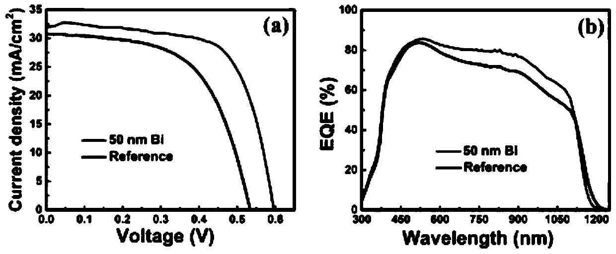
[0053] This embodiment provides a compound thin film solar cell, which is prepared by the following method:
[0054] S1: Using molybdenum-coated soda-lime glass as the substrate, a 50nm-thick Bi layer was deposited on the Mo surface by DC sputtering a metal Bi target. The Bi target was a circular target with a diameter of 3 inches and a thickness of 5mm. During the sputtering process, Ar is introduced as the working gas, the sputtering pressure is 0.8Pa, and the sputtering power density is 0.679W / cm 2 , sputtering time 20s;
[0055] S2: The CIGS precursor is prepared by radio frequency magnetron sputtering quaternary target. The quaternary target contains Cu, In, Ga and Se at the same time. The atomic ratio is: 22:17.5:7.5:53. The target The size of the material is the same as that of the Bi target. After the preparation is completed, sputter deposition is carried out. During the sputtering process, the sputtering pressure is 1.0Pa, and the sputtering power density is 3.395W...
Embodiment 2
[0062] Example 2 provides a compound thin film solar cell, the difference between its preparation method and Reference Document 1 is that in this example:
[0063] The thickness of the metal Bi layer is selected to be 100 nm, the thickness of the absorbing layer is selected to be 2 μm, the annealing temperature rise rate is 30° C. / min, the annealing time is 60 minutes, and the annealing temperature is 500° C.
PUM
| Property | Measurement | Unit |
|---|---|---|
| Thickness | aaaaa | aaaaa |
| Thickness | aaaaa | aaaaa |
| Thickness | aaaaa | aaaaa |
Abstract
Description
Claims
Application Information
 - R&D
- Intellectual Property
- Life Sciences
- Materials
- Tech Scout
- Unparalleled Data Quality
- Higher Quality Content
- 60% Fewer Hallucinations
Browse by: Latest US Patents, China's latest patents, Technical Efficacy Thesaurus, Application Domain, Technology Topic, Popular Technical Reports.
© 2025 PatSnap. All rights reserved.Legal|Privacy policy|Modern Slavery Act Transparency Statement|Sitemap|About US| Contact US: help@patsnap.com


