Bionic synaptic device, manufacturing method and application thereof

A synaptic device and synaptic technology, applied in the direction of electrical components, etc., can solve the problems of high working voltage, lack of dynamic learning and memory ability, etc.

Active Publication Date: 2020-01-31
NINGBO INST OF MATERIALS TECH & ENG CHINESE ACADEMY OF SCI
View PDF3 Cites 10 Cited by
  • Summary
  • Abstract
  • Description
  • Claims
  • Application Information

AI Technical Summary

Problems solved by technology

However, due to the limitation of the device structure and gate dielectric material, the traditional oxide th...

Method used


Image

  • Bionic synaptic device, manufacturing method and application thereof
  • Bionic synaptic device, manufacturing method and application thereof
  • Bionic synaptic device, manufacturing method and application thereof

Examples


Embodiment 1

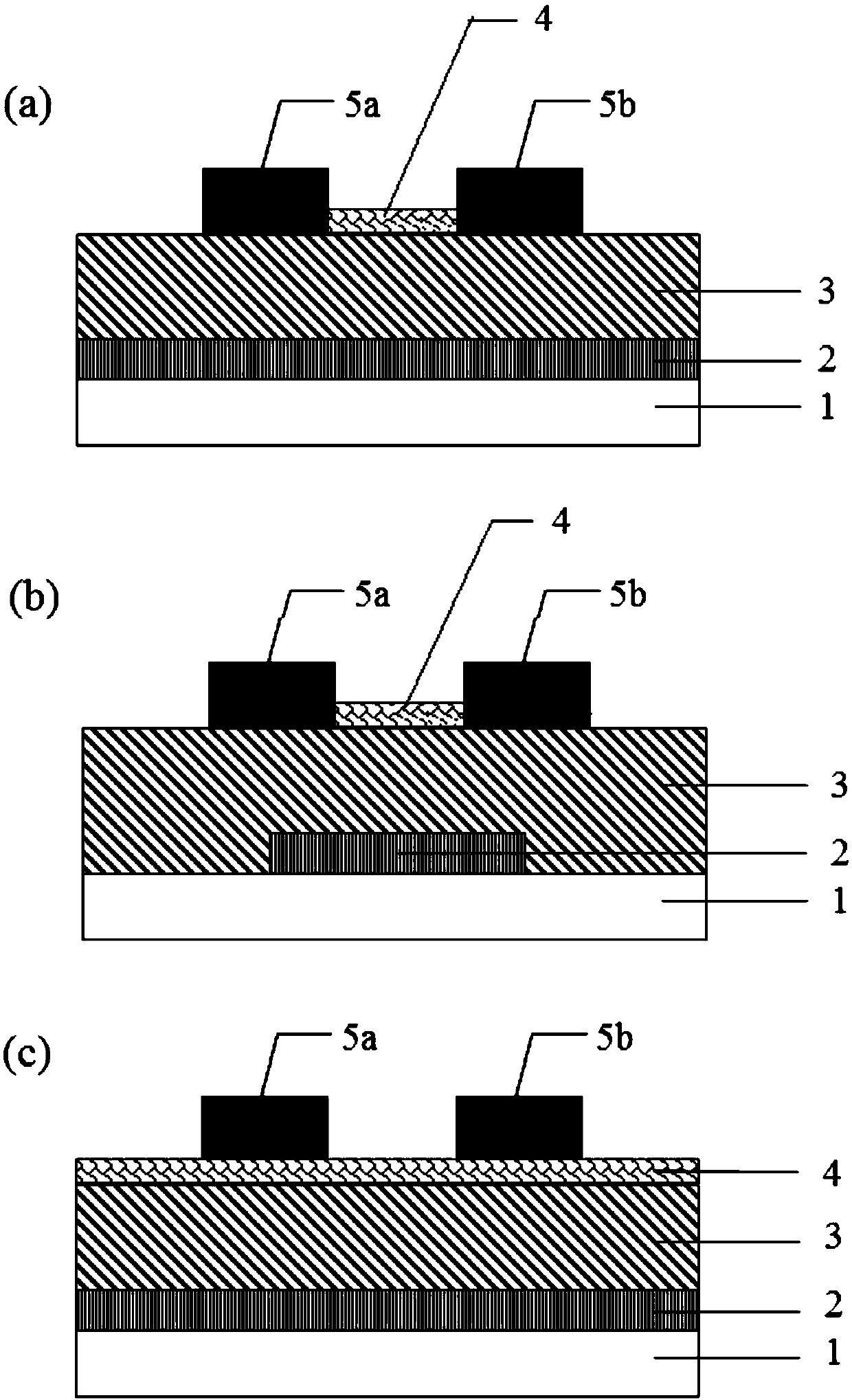
[0180] In this example, if figure 1 As shown in (a), glass substrate is selected as insulating substrate 1, indium tin oxide film (InSnO) is selected as conductive layer 2, chitosan film is selected as gate dielectric layer 3, and indium tin oxide film (InSnO) is selected as channel layer 4. ).

[0181] The manufacturing method of the oxide biomimetic synapse device comprises the following steps:

[0182] Step 1: Clean the glass substrate sequentially with alcohol and deionized water ultrasonically and dry it with a nitrogen gun, then deposit an InSnO thin film conductive layer 2 on the surface of the glass substrate 1;

[0183] Step 2: On the conductive layer 2, prepare a chitosan film 3 by spin coating, and the thickness of the chitosan grid dielectric film is 12 microns;

[0184] Step 3: On the chitosan film 3, use magnetron sputtering technology to deposit patterned InSnO channel layer 4, and form patterned InSnO source and drain electrodes 5a and 5b on both sides of th...

Embodiment 2

[0187] In this example, if figure 1 As shown in (b), a plastic substrate is selected for the insulating substrate 1, an indium zinc oxide film (InZnO) is selected for the conductive layer 2, a porous silicon dioxide film is selected for the gate dielectric layer 3, and an indium zinc oxide film (InZnO) is selected for the channel layer 4 ( InZnO).

[0188] The manufacturing method of the oxide biomimetic synapse device comprises the following steps:

[0189] Step 1: ultrasonically clean the plastic substrate with alcohol and deionized water in sequence and dry it with a nitrogen gun, and then deposit a patterned InZnO thin film conductive layer 2 on the surface of the plastic substrate 6;

[0190] Step 2: On the conductive layer 2, a porous silicon dioxide particle gate dielectric film 3 is deposited by plasma-enhanced chemical vapor deposition (PECVD), and the thickness of the porous silicon dioxide particle film is 2 microns;

[0191] Step 3: On the porous silicon dioxide...

Embodiment 3

[0194] In this example, if figure 1 As shown in (c), polyimide substrate is selected for insulating substrate 1, aluminum zinc oxide film (AZO) is selected for conductive layer 2, sodium alginate film is selected for gate dielectric layer 3, and indium tungsten oxide is selected for channel layer 4 thin film (InWO).

[0195] The manufacturing method of the oxide biomimetic synapse device comprises the following steps:

[0196] Step 1: ultrasonically clean the polyimide substrate with alcohol and deionized water in sequence and dry it with a nitrogen gun, and then deposit an aluminum zinc oxide film (AZO) conductive layer 2 on the surface of the polyimide substrate 1;

[0197] Step 2: On the conductive layer 2, prepare a sodium alginate film 3 by spin coating, the thickness of the sodium alginate film is 8 microns, as a gate dielectric layer;

[0198] Step 3: On the sodium alginate gate dielectric film 3, deposit an indium tungsten oxide film (InWO) as a channel layer 4 by m...


PUM

PropertyMeasurementUnit
Sheet resistanceaaaaaaaaaa
Carrier concentrationaaaaaaaaaa
Conductivityaaaaaaaaaa

Abstract

The invention discloses a bionic synaptic device and a manufacturing method and application thereof. Specifically, the invention relates to the bionic synaptic device with spike-time-dependent plasticity learning behaviors. The bionic synaptic device includes a gate electrode (2), wherein the square resistance of the gate electrode is 30 to 800 omega. The gate electrode is used as the synaptic front end of the bionic synaptic device. The device further includes a gate dielectric layer (3) which comprises a solid electrolyte with a proton conductive property, a channel (4), wherein the channellayer is used as the synaptic rear end of the bionic synaptic device. The device further includes a source (5a) and a drain (5b). According to the bionic synaptic device, different linear spike-time-dependent plasticity learning behaviors can be realized on a single device; the circuit design is greatly simplified; and the device has important application prospects in the fields of neuromorphic devices, artificial intelligence and the like.

Description

technical field [0001] The invention relates to the technical field of artificial intelligence, in particular to an oxide biomimetic synapse device with spike time-dependent plasticity (STDP) learning behavior, a manufacturing method and an application thereof. Background technique [0002] Artificial intelligence has evolved over the decades since John McCarthy coined the term "artificial intelligence (AI)" in the 1950s to mimic the way the human brain works. In recent years, with the advent of the era of big data, and with the development of microelectronics technology and the advancement of computer technology, especially after the launch of "AlphaGo", AI technology has attracted more and more people's attention, and it will affect people's production have a huge impact on lifestyles. However, it is worth noting that the current AI technology is mainly realized by using the von Neumann structure combined with the optimization of the artificial neural network algorithm. ...

Claims


Application Information

Patent Timeline
IPC IPC(8): H01L45/00
CPCH10N70/253H10N70/841H10N70/011
Inventor 竺立强虞菲肖惠
Owner NINGBO INST OF MATERIALS TECH & ENG CHINESE ACADEMY OF SCI
Why Eureka
Try Eureka