A kind of memristor and preparation method thereof

A memristor and low-resistance silicon substrate technology, which is applied in the field of micro-nano processing of semiconductor devices, can solve the problem that the magnitude of change of the high and low resistance of the memristor is not obvious, it is not easy to control the on and off state of the memristor, and the deposited film is not stable. Continuous and other issues, to achieve the effects of obvious on and off states, low cost, and good application benefits

Active Publication Date: 2021-11-09
UNIV OF ELECTRONICS SCI & TECH OF CHINA
View PDF5 Cites 0 Cited by
  • Summary
  • Abstract
  • Description
  • Claims
  • Application Information

AI Technical Summary

Problems solved by technology

However, most of the memristor structures currently used are planar structures. After the bias voltage is applied, the magnitude of the high and low resistance changes of the memristor is not obvious, which makes it difficult to control the on and off states of the memristor well.
Furthermore, in the existing methods for preparing memristors, there are some problems in actually forming a suitable memristor structure and depositing thin films. Poor performance leads to problems such as easy direct short-circuit of the top and bottom layers after the voltage is applied, and a method for preparing a large-area high-performance memristor of the present invention aims to solve and improve the above-mentioned problems

Method used


Image

  • A kind of memristor and preparation method thereof
  • A kind of memristor and preparation method thereof
  • A kind of memristor and preparation method thereof

Examples


Embodiment 1

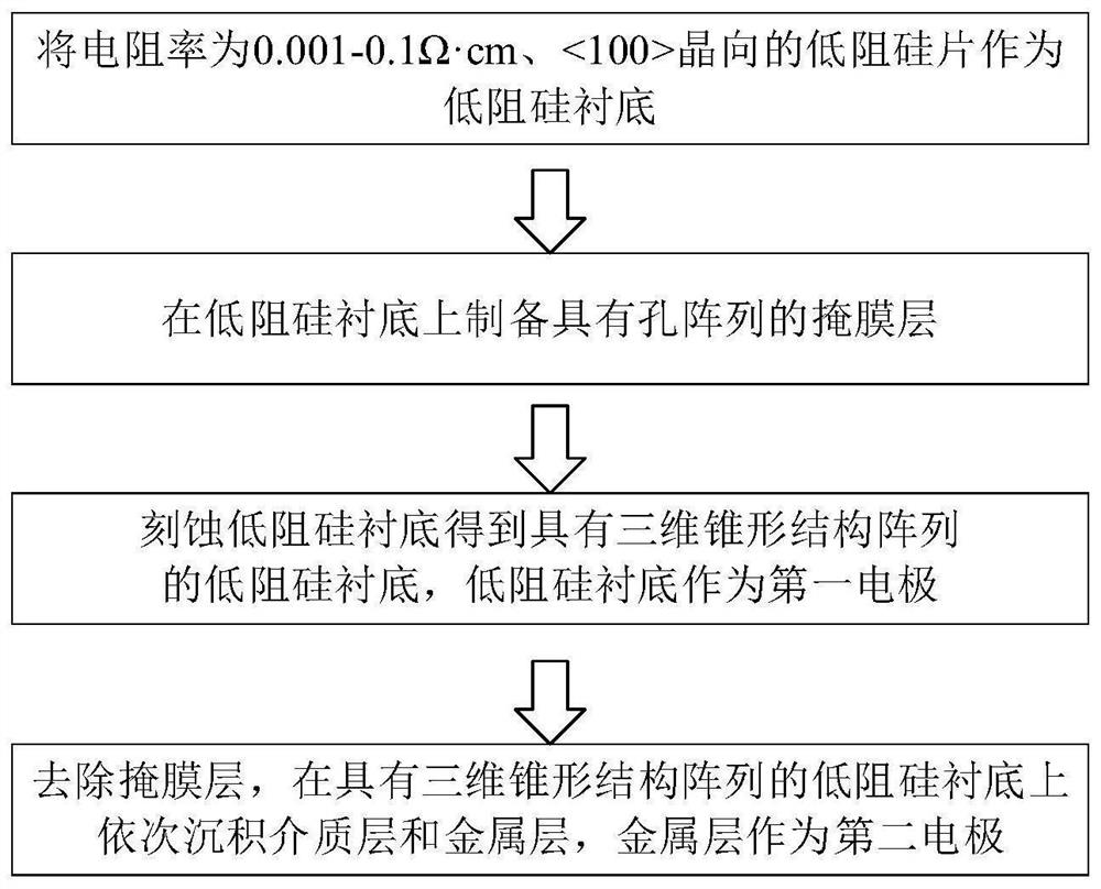
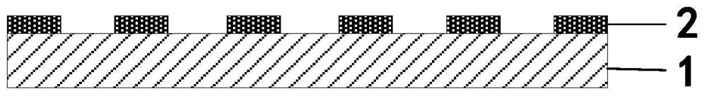
[0040] Such as figure 1 Shown, in embodiment 1, a kind of memristor preparation method specifically comprises the following steps:

[0041] S01: Prepare a dry and polished low-resistance silicon substrate with a resistivity less than 0.01Ω·cm as the low-resistance silicon substrate 1;

[0042] S02: Prepare a hole array patterned mask layer 2 on a low-resistance silicon substrate 1; specifically, an ordered mask layer 2 can be obtained by spin-coating a photoresist on the silicon surface, and exposing and developing by using double-beam interference lithography. Disc array photoresist pattern, and then deposit an etching mask layer 2 (wet etching protective layer) on the sample, specifically: spin-coat SXAR-P3500 / 6 positive photolithography on a low-resistance silicon substrate 1 The ratio of photoresist and diluent is 1:1.5 (volume ratio), uniform glue for 30s at a speed of 4000rpm (rotation per minute), to obtain a glue thickness of 230nm, and use double-beam interference p...

Embodiment 2

[0048] This embodiment has the same inventive concept as Embodiment 1, and provides a method for preparing a memristor. The method specifically includes the following steps:

[0049] S11: Prepare a dry and polished low-resistance silicon substrate with a resistivity of 0.01Ω·cm as the low-resistance silicon substrate 1;

[0050] S12: The cleaned and dried low-resistance silicon substrate 1 is sequentially treated with polydiallyldimethylammonium chloride (PDDA, 4%), deionized water, and blown dry with a nitrogen gun; Sodium xanthate (PSS, 3%), deionized water treatment, nitrogen gun blow-dry, then through amyl xanthate potassium (PAX, 2%) and deionized water treatment, nitrogen gun blow-dry, obtain surface has positive charge 1 sample of low-resistance silicon substrate;

[0051] S13: Drop a solution of colloidal balls with a diameter of 500nm (0.5% by mass fraction of microspheres) on the surface of the low-resistance silicon substrate 1 sample sheet in step S12, the colloi...

Embodiment 3

[0057] This embodiment has the same inventive concept as Embodiment 1 and Embodiment 2, and provides a method for preparing a memristor. The method specifically includes the following steps:

[0058] S21: Prepare a dry and polished low-resistance silicon substrate with a resistivity of 0.01Ω·cm as the low-resistance silicon substrate 1;

[0059] S22: Use 5ml of 800nm ​​PS microspheres with 5% w / v, add 0.15ml of absolute ethanol, and assemble the closely arranged PS microspheres on the silicon wafer by the air-liquid surface assembly method;

[0060] S23: performing reactive ion etching on the sample sheet (performed in an oxygen environment), so that the closely arranged array of PS microspheres becomes a non-closely arranged array. The reaction rate can be adjusted by changing the power and the gas rate. For example, at 80W, 60mTorr gas pressure, the rate of oxygen gas is 120sccm, and the diameter of microspheres with a diameter of 800nm ​​is reduced to 550nm after being etc...


PUM

PropertyMeasurementUnit
electrical resistivityaaaaaaaaaa
thicknessaaaaaaaaaa

Abstract

The invention discloses a memristor and a preparation method thereof, which belong to the technical field of micro-nano processing of semiconductor devices. The method comprises using a low-resistance silicon chip whose resistivity satisfies the first threshold condition and whose crystal orientation is <100> as a low-resistance silicon lining. bottom; prepare a mask layer with hole arrays on the low-resistance silicon substrate; etch the low-resistance silicon substrate to obtain a low-resistance silicon substrate with a three-dimensional cone structure array, the three-dimensional cone structure The low-resistance silicon substrate of the array is used as the first electrode layer; the mask layer is removed, and a dielectric layer and a metal layer are sequentially deposited on the low-resistance silicon substrate with a three-dimensional tapered structure array, and the metal layer is used as the second electrode layer. Two electrode layers. The invention introduces a three-dimensional tapered structure array into both the low-resistance silicon substrate and the metal layer, so that the on and off states of the memristor are more obvious and easier to control, and the low-resistance silicon substrate is directly used as the lower electrode, reducing the The memristor film layer reduces the probability of leakage of the memristor and increases the area of ​​the memristor array.

Description

technical field [0001] The invention relates to the technical field of micro-nano processing of semiconductor devices, in particular to a method for rapidly manufacturing a large-area memristor array and the memristor. Background technique [0002] Information is an important resource in today's society. As a storage carrier for information, storage devices are one of the core components of various electronic devices. However, the current storage devices have encountered unprecedented challenges: on the one hand, the size of semiconductor transistors has shrunk, and the storage capacity and read / write speed have reached their physical limits, accompanied by phenomena such as chip heating, and the stability decreases with time; on the other hand On the one hand, the increase in the cost of dense lithography and the defects of the device itself have hindered the development of integrated circuit technology. Therefore, it is urgent to explore a new memory device with high spee...

Claims


Application Information

Patent Timeline
Patent Type & Authority Patents(China)
IPC IPC(8): H01L45/00
CPCH10N70/821H10N70/066
Inventor 王军刘贤超崔官豪周泓希苟军史佳欣刘德幸
Owner UNIV OF ELECTRONICS SCI & TECH OF CHINA
Why Eureka
Try Eureka