Surface plasmon enhanced InGaN/GaN multi-quantum well photoelectrode and production method thereof

A surface plasmon, multiple quantum well technology, applied in the field of solar cells, can solve the problems of accelerating the separation of electron-hole pairs and not much research, and achieve the effect of improving light absorption capacity, improving efficiency, and increasing the rate of production

Active Publication Date: 2020-02-25
GX OPTOELECTRONIC TECH INST CO LTD
View PDF16 Cites 8 Cited by
  • Summary
  • Abstract
  • Description
  • Claims
  • Application Information

AI Technical Summary

Problems solved by technology

[0004] There are many studies on surface plasmon-enhanced solar photoelectrochemical cell efficiency, but there are not many studies on the coupling of InGaN-based semiconductor materials and plasmonic metals. How to use the plasmon effect to increase InGaN / GaN multi-quantum well solar energy It is a difficult point to accelerate the separation of electron-hole pairs by using the built-in electric field formed by the high doping concentration of the p-n region while maintaining the efficiency of photoelectrochemical cells.

Method used


Image

  • Surface plasmon enhanced InGaN/GaN multi-quantum well photoelectrode and production method thereof
  • Surface plasmon enhanced InGaN/GaN multi-quantum well photoelectrode and production method thereof
  • Surface plasmon enhanced InGaN/GaN multi-quantum well photoelectrode and production method thereof

Examples


Embodiment 1

[0050] The preparation method of this solar photoelectrochemical cell, its step comprises:

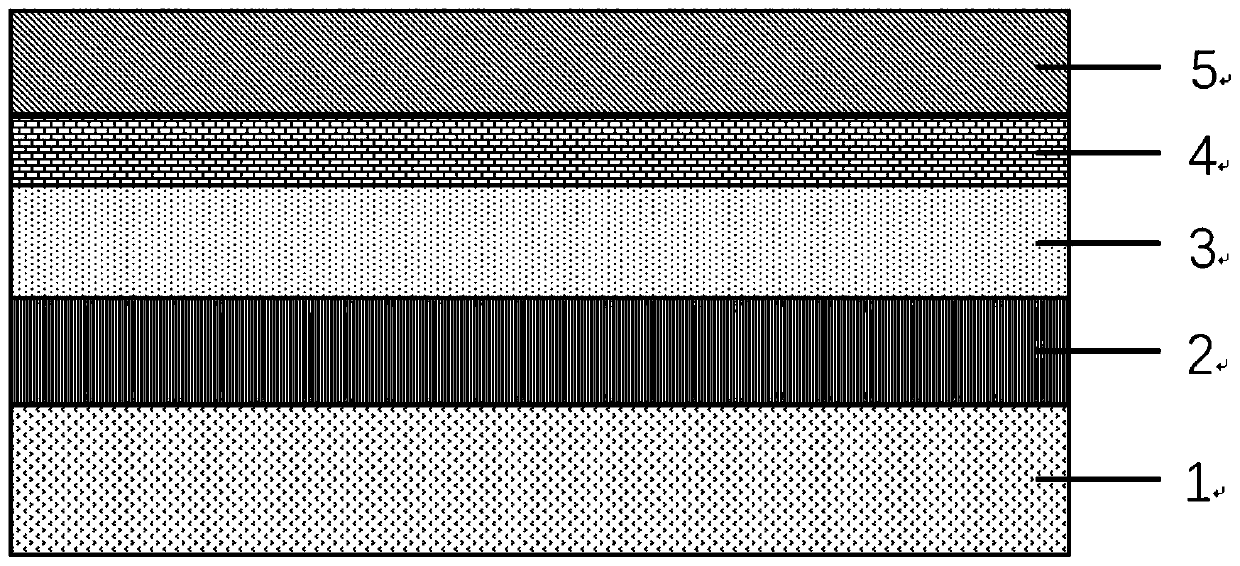
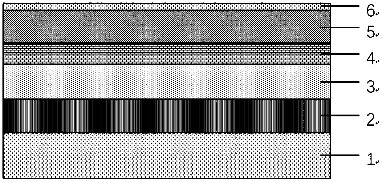
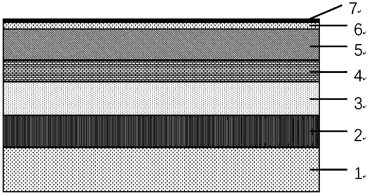
[0051] A1, the InGaN / GaN multi-quantum well LED substrate (such as an InGaN / GaN multi-quantum well LED substrate with an In composition of 0.3, an emission wavelength of 510nm, and a quantum well period of 10 figure 1 As shown, it includes an n-type GaN layer 3 with a thickness of 2 μm, an In layer with a period number of 10 and a thickness of 150 nm x Ga 1-x N / GaN quantum well active layer 4 (the thickness of the InGaN well layer is 3nm, the thickness of the GaN barrier layer is 12nm) and the p-type GaN layer 5 with a thickness of 500nm) grows a layer of 200nm thick SiO 2 Dielectric film layer 6, such as figure 2 As shown, a 10nm thick Ni metal film layer 7 was vapor-deposited on SiO 2 The surface of layer dielectric film 6, such as image 3 shown;

[0052] A2. Using rapid thermal annealing technology, anneal the sample obtained in step A for 3 minutes at 850°C under a nitrogen ...


PUM

PropertyMeasurementUnit
diameteraaaaaaaaaa
thicknessaaaaaaaaaa
diameteraaaaaaaaaa

Abstract

The invention discloses a surface plasmon enhanced InGaN / GaN multi-quantum well photoelectrode. A substrate is etached to form a nanorod structure penetrating through a p-GaN layer and going deep to amulti-quantum well active layer, and plasmon metal is filled in the position of the multi-quantum well active layer between nanorods. The invention also discloses an application of the electrode as aworking electrode of a solar photoelectrochemical cell, the produced solar photoelectrochemical cell and a production method of the solar photoelectrochemical cell. A top-down etching technology of aself-assembled Ni mask is adopted to regulate a distance between the plasma metal and the multi-quantum well in order to generate near field coupling, and the efficiency of generation and transportation of electron hole pairs on the surface of the multi-quantum well active region is effectively improved under the combined action of an electromagnetic field generated by the surface plasmon effectand a built-in electric field formed by the high doping concentration of the p-n region. The method is suitable for InGaN type photoelectrode materials with adjustable band gaps and matched with solarspectra.

Description

technical field [0001] The invention relates to a surface plasmon-enhanced InGaN / GaN multi-quantum well photoelectrode, a solar photoelectrochemical cell made by using a surface plasmon-enhanced InGaN / GaN multi-quantum well photoelectrode and a preparation method thereof, belonging to The field of solar cell technology. Background technique [0002] With the rapid growth of population and economy, coal, oil, natural gas and other fossil fuels have become increasingly depleted with the intensification of development. If things go on like this, they will not be able to meet the energy needs of people's lives. Therefore, looking for new alternative energy has become the future of mankind. urgent task of development. As a green, low-carbon and environmentally friendly renewable energy, solar energy has become one of the most potential energy sources among many emerging energy sources. But so far, the utilization efficiency of solar energy is still very low, and there are certa...

Claims


Application Information

Patent Timeline
Patent Type & Authority Applications(China)
IPC IPC(8): C25B11/06C25B1/04C23C14/24C23C14/18C23C14/58C23C16/40C23C16/50C23C16/56B82Y10/00B82Y30/00
CPCB82Y10/00B82Y30/00C23C14/18C23C14/24C23C14/5806C23C16/402C23C16/50C23C16/56C25B1/04C25B1/55C25B11/051C25B11/091Y02E60/36Y02P20/133
Inventor 谢自力桑艺萌刘斌
Owner GX OPTOELECTRONIC TECH INST CO LTD
Why Eureka
Try Eureka