Enhanced silicon carbide MOSFET device and manufacturing method thereof

A manufacturing method and technology of silicon carbide, which are applied in semiconductor/solid-state device manufacturing, semiconductor devices, electric solid-state devices, etc., can solve the problems of reducing the current driving capability of the device, high PN diode turn-on voltage, and high forbidden band width, and reduce the interface. Effects of damage, elimination of JFET effects, and enhancement of current capability

Active Publication Date: 2020-04-28
SOUTH UNIVERSITY OF SCIENCE AND TECHNOLOGY OF CHINA
View PDF8 Cites 12 Cited by
  • Summary
  • Abstract
  • Description
  • Claims
  • Application Information

AI Technical Summary

Problems solved by technology

Due to the high band gap of the SiC material, the turn-on voltage of the anti-parallel PN diode is very high, and the corresponding loss is also large.
[0006] 2. The anti-parallel PN diodes in the prior art reduce the current drive capability of the device and also increase the loss

Method used


Image

  • Enhanced silicon carbide MOSFET device and manufacturing method thereof
  • Enhanced silicon carbide MOSFET device and manufacturing method thereof
  • Enhanced silicon carbide MOSFET device and manufacturing method thereof

Examples


Embodiment Construction

[0056] The subject matter of the invention will now be discussed with reference to several exemplary embodiments. It should be understood that these embodiments are discussed only to enable those of ordinary skill in the art to better understand and thus implement the content of the present invention, and do not imply any limitation on the scope of the present invention.

[0057] As used herein, the term "comprising" and variations thereof are to be read as open-ended terms meaning "including but not limited to". The term "based on" is to be read as "based at least in part on". The terms "one embodiment" and "an embodiment" are to be read as "at least one embodiment". The term "another embodiment" is to be read as "at least one other embodiment".

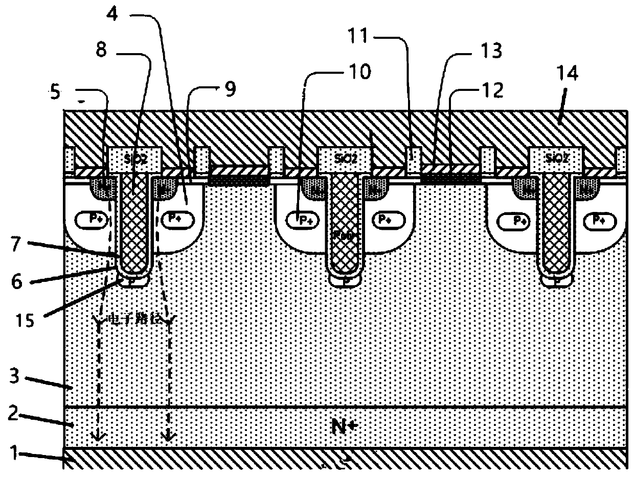
[0058] The invention provides an enhanced silicon carbide MOSFET device and a manufacturing method aiming at increasing the turn-on voltage of the device and reducing the current driving capability of the device in the prior art w...


PUM

PropertyMeasurementUnit
thicknessaaaaaaaaaa
thicknessaaaaaaaaaa
depthaaaaaaaaaa

Abstract

The invention discloses an enhanced silicon carbide MOSFET device. The enhanced silicon carbide MOSFET device sequentially comprises back metal, an N+ type heavily doped SiC substrate, an N- epitaxiallayer, an insulating dielectric layer and front metal from bottom to top. According to the invention, a Schottky diode is integrated into the MOSFET device, and the area of a Schottky barrier metal layer is flexibly increased or decreased to adjust and adapt to the current and specification of the MOSFET and the Schottky diode, so that the effects of increasing the switching speed of the MOSFET,reducing the switching loss and the like are achieved, the performance and the reliability of the device can be greatly improved, and the application cost of the device is reduced. The enhanced silicon carbide MOSFET device adopts a trench SiC MOSFET design, and a conductive channel is changed from the traditional horizontal direction to the vertical direction, so that a JFET effect between primitive cells of the traditional MOSFET is eliminated, and the current capability of the device is improved. The gate bottom P region at the bottom of the trench can protect and weaken an electric field at the bottom of the trench, thereby playing a certain role in electrostatic shielding of gate oxide at the bottom of the trench, and improving the reliability of the device. Meanwhile, certain help isprovided for voltage resistance of the device.

Description

technical field [0001] The invention belongs to the technical field of semiconductor chip manufacturing technology, and in particular relates to an enhanced silicon carbide MOSFET device and a manufacturing method thereof. Background technique [0002] The third-generation semiconductor material silicon carbide (SiC) has many characteristics different from traditional silicon semiconductor materials. Its energy band gap is 2.8 times that of silicon, reaching 3.09 electron volts; its insulation breakdown field strength is 5.3 times that of silicon, up to 3.2 MV / cm, its thermal conductivity is 3.3 times that of silicon, which is 49w / cm·K. This makes it an ideal semiconductor material for high temperature, high frequency, high power, and radiation-resistant applications. Since silicon carbide power devices can significantly reduce the energy consumption of electronic equipment, silicon carbide power devices have been widely used in the field of new energy. [0003] Metal-Oxid...

Claims


Application Information

Patent Timeline
Patent Type & Authority Applications(China)
IPC IPC(8): H01L29/06H01L29/423H01L29/45H01L29/47H01L29/78H01L29/872H01L27/06H01L21/04H01L21/82H01L21/28H01L21/336H01L21/329
CPCH01L27/0629H01L21/8213H01L29/7827H01L29/66068H01L29/0623H01L29/872H01L29/6606H01L29/47H01L29/4236H01L29/401H01L29/45H01L21/0495H01L21/0485
Inventor 吴苏州李晓云杨高洁叶怀宇张国旗
Owner SOUTH UNIVERSITY OF SCIENCE AND TECHNOLOGY OF CHINA
Why Eureka
Try Eureka