
Alkali metal doping treatment method for large-scale production of copper-indium-gallium-selenium thin-film solar cell

A technology of solar cells and copper indium gallium selenide, applied in circuits, photovoltaic power generation, electrical components, etc., can solve problems such as long return time, hydrogen selenide generation, time-consuming disadvantages, etc., to reduce surface roughness and increase open circuit voltage , the effect of reducing the annealing time

Active Publication Date: 2020-06-02
ZHEJIANG SHANGYUE OPTOELECTRONICS TECH +1
View PDF4 Cites 1 Cited by
  • Summary
  • Abstract
  • Description
  • Claims
  • Application Information

AI Technical Summary

Problems solved by technology

[0010] (3) Alkali metal doping after the deposition of CIGS absorption layer on flexible substrates requires two processes, and requires a long return time, and the complex and time-consuming process is not conducive to large-scale production
[0011] Since some alkali metal materials are easy to absorb water during the addition process, this will cause some hydrogen selenide to be generated during the doping process of alkali metals. After opening the cavity, if excessive hydrogen selenide is inhaled, it will easily cause poisoning symptoms and cause safety problems.

Method used


Image

  • Alkali metal doping treatment method for large-scale production of copper-indium-gallium-selenium thin-film solar cell
  • Alkali metal doping treatment method for large-scale production of copper-indium-gallium-selenium thin-film solar cell
  • Alkali metal doping treatment method for large-scale production of copper-indium-gallium-selenium thin-film solar cell

Examples


Embodiment 1

[0058] An alkali metal doping treatment method for large-scale production of copper indium gallium selenide thin film solar cells, the steps are as follows:

[0059] 1. On a flexible film substrate (stainless steel) with a thickness of 25 μm, a 0.4 μm thick Mo back electrode layer was deposited on the substrate by DC magnetron sputtering.

[0060] 2. Add 1700g of silica gel desiccant in the reaction equipment as a water absorbent, and the vacuum degree is 1×10 -3 In the co-evaporation chamber of Pa, the substrate is heated to 150°C, and a layer of NaF is evaporated on the surface of the Mo back electrode layer. The temperature of the NaF evaporation source is 760-800°C, and the evaporation time is 10min.

[0061] 3. Raise the temperature of the substrate to 480°C, and co-evaporate In, Ga, and Se. The temperature of the In evaporation source is 940-1050°C, the temperature of the Ga evaporation source is 1050-1200°C, and the temperature of the Se evaporation source is 450-500°C....

Embodiment 2

[0072] An alkali metal doping treatment method for large-scale production of copper indium gallium selenide thin film solar cells, the steps are as follows:

[0073] 1. On a flexible film substrate (polyimide) with a thickness of 40 μm, a 0.8 μm thick Mo back electrode layer was deposited on the substrate by DC magnetron sputtering.

[0074] 2. Add 1800g of anhydrous calcium chloride in the reaction equipment as a water-absorbing agent, and the vacuum degree is 3×10 -3 In the co-evaporation chamber of Pa, the substrate is heated to 300°C, and a layer of NaF is evaporated on the surface of the Mo back electrode layer. The temperature of the NaF evaporation source is 760-800°C, and the evaporation time is 20min.

[0075] 3. Increase the temperature of the substrate to 600°C, and co-evaporate In, Ga, and Se, where the temperature of the In evaporation source is 940-1050°C, the temperature of the Ga evaporation source is 1050-1200°C, and the temperature of the Se evaporation sourc...

Embodiment 3

[0086] An alkali metal doping treatment method for large-scale production of copper indium gallium selenide thin film solar cells, the steps are as follows:

[0087] 1. On a flexible film substrate (stainless steel) with a thickness of 30 μm, a 0.6 μm thick Mo back electrode layer was deposited on the substrate by DC magnetron sputtering.

[0088] 2. Add 2000g of silica gel desiccant to the reaction equipment as a water absorbent, and the vacuum degree is 2×10 -3 In the co-evaporation chamber of Pa, the substrate is heated to 200°C, and a layer of NaF is evaporated on the surface of the Mo back electrode layer. The temperature of the NaF evaporation source is 760-800°C, and the evaporation time is 15min.

[0089] 3. Raise the temperature of the substrate to 550°C, and co-evaporate In, Ga, and Se. The temperature of the In evaporation source is 940-1050°C, the temperature of the Ga evaporation source is 1050-1200°C, and the temperature of the Se evaporation source is 450-500°C....


PUM

PropertyMeasurementUnit
thicknessaaaaaaaaaa
thicknessaaaaaaaaaa
thicknessaaaaaaaaaa

Abstract

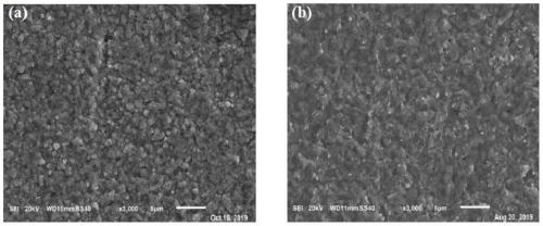
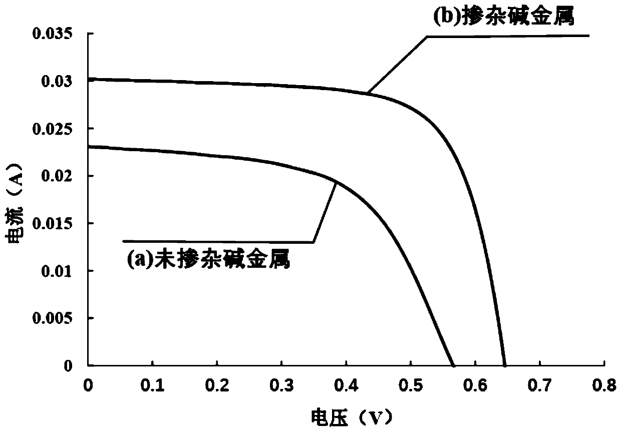
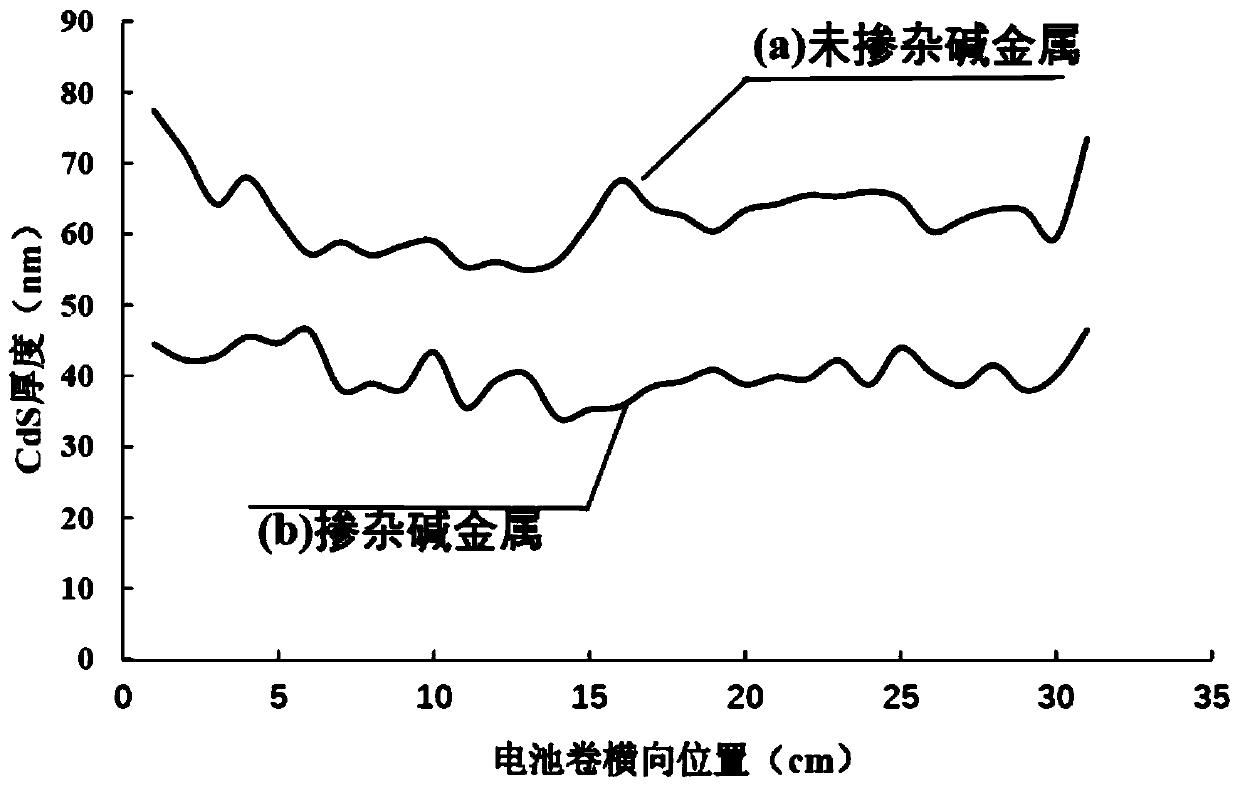
The invention discloses an alkali metal doping treatment method for large-scale production of a copper-indium-gallium-selenium thin-film solar cell. The method sequentially comprises the following steps: (1) depositing a Mo back electrode layer; (2) depositing a layer of alkali metal halide; (3) co-evaporating In, Ga and sixth main group solid elementary substances; (4) co-evaporating Cu and sixthmain group solid elementary substances; (5) depositing a layer of alkali metal halide; (6) co-evaporating Cu and sixth main group solid elementary substances; (7) co-evaporating In, Ga and sixth maingroup solid elementary substances; (8) depositing a layer of alkali metal halide; (9) performing annealing treatment. According to the method, the adhesive force of the Mo layer and the CIGS layer can be effectively increased, the CIGS hole concentration is increased, the surface roughness of the thin film is reduced, the thickness of the CdS buffer layer is reduced, and the open-circuit voltageand the photoelectric conversion efficiency of the thin film solar cell are improved.

Description

technical field [0001] The invention relates to the technical field of thin film photovoltaic device production, in particular to an alkali metal doping treatment method for large-scale production of copper indium gallium selenium thin film solar cells. Background technique [0002] As a clean energy, solar energy has developed rapidly in recent years. The installed capacity of solar cells has been increasing at an annual growth rate of nearly 25%. By 2017, the global cumulative installed capacity has exceeded 402.5GW, showing a good momentum of development. According to the forecast of the International Energy Agency (IEA), the cumulative installed capacity of photovoltaics in the world is expected to reach 1721GW by 2030, and will rise to 4670GW by 2050. The development potential of the photovoltaic industry is huge. [0003] High-efficiency thin-film solar cells with copper indium gallium selenide as the absorption layer are collectively referred to as copper indium galli...

Claims


Application Information

Patent Timeline
Patent Type & Authority Applications(China)
IPC IPC(8): H01L31/18
CPCH01L31/18H01L31/186H01L31/1864Y02E10/50Y02P70/50
Inventor 胡煜霖刘宽菲任宇航
Owner ZHEJIANG SHANGYUE OPTOELECTRONICS TECH
Learn More