MSM type alpha-Ga2O3 based solar blind ultraviolet light detector
A -ga2o3, detector technology, applied in the field of MSM type α-Ga2O3-based sun-blind ultraviolet light detectors and its preparation, can solve the problems of crystal quality decline, lower device electrical performance and stability, etc., and achieve stable and good performance Detection ability, effect of high light-to-dark current ratio
- Summary
- Abstract
- Description
- Claims
- Application Information
AI Technical Summary
Problems solved by technology
Method used
Image
Examples
Embodiment 1
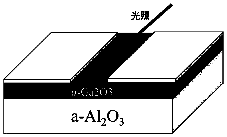
[0055] Such as figure 1 As shown, a kind of MSM type α-Ga of this embodiment 2 o 3 A solar-blind ultraviolet photodetector, the detector comprises an a-plane sapphire substrate, an active layer, and a pair of parallel metal electrodes from bottom to top, wherein: the active layer is (110)-oriented α-Ga 2 o 3 thin film, the material of the parallel metal electrodes is Au, the thickness of the substrate is 0.43 mm, the thickness of the active layer is 120 nm, the thickness of the parallel metal electrodes is 50 nm, and the distance between the parallel metal electrodes is 10 μm .
[0056] The MSM type α-Ga mentioned above in this embodiment 2 o 3 The base sun-blind ultraviolet light detector is prepared by the following method, including the following steps:
[0057] Step 1: Preparation of Ga by sintering by solid phase sintering method 2 o 3 Ceramic target
[0058] 1.1 Weigh 10~15g Ga 2 o 3 Powder, add ultra-pure water, mix evenly, put it in a ball mill jar and weigh...
Embodiment 2
[0067] Embodiment 2 (comparative example)
[0068] A kind of MSM type amorphous α-Ga of this embodiment 2 o 3 A base sun-blind ultraviolet light detector, the detector includes an a-plane sapphire substrate, an active layer, and a pair of parallel metal electrodes from bottom to top, wherein: the active layer is amorphous Ga 2 o 3 thin film, the material of the parallel metal electrodes is Au, the thickness of the substrate is 0.43 mm, the thickness of the active layer is 120 nm, the thickness of the parallel metal electrodes is 55 nm, and the distance between the parallel metal electrodes is 10 μm .
[0069] The MSM type amorphous α-Ga mentioned above in this embodiment 2 o 3 The base sun-blind ultraviolet light detector is prepared by the following method, including the following steps:
[0070] Step 1 utilizes the Ga in embodiment 1 2 o 3 Fabrication of solar-blind ultraviolet light detectors with ceramic targets
[0071] 1.1 Ga prepared in step 1 2 o 3 The ceram...
Embodiment 3
[0075] Embodiment 3 (comparative example)
[0076] A kind of MSM type β-Ga of this embodiment 2 o 3 A solar-blind ultraviolet photodetector, which includes a c-plane sapphire substrate, an active layer, and a pair of parallel metal electrodes from bottom to top, wherein: the active layer is β-Ga 2 o 3 thin film, the material of the parallel metal electrodes is Au, the thickness of the substrate is 0.43 mm, the thickness of the active layer is 150 nm, the thickness of the parallel metal electrodes is 55 nm, and the distance between the parallel metal electrodes is 10 μm .
[0077] The MSM type β-Ga mentioned above in this embodiment 2 o 3 The base sun-blind ultraviolet light detector is prepared by the following method, including the following steps:
[0078] Step 1: Preparation of Ga by sintering by solid phase sintering method 2 o 3 Ceramic target
[0079] 1.1 Weigh 10g Ga 2 o 3 Powder, add 15g of deionized water, then place in the ball mill jar (the ball milling m...
PUM
| Property | Measurement | Unit |
|---|---|---|
| thickness | aaaaa | aaaaa |
| thickness | aaaaa | aaaaa |
| thickness | aaaaa | aaaaa |
Abstract
Description
Claims
Application Information


