

PERL solar cell with double-sided power generation and preparation method of PERL solar cell
A solar cell, double-sided technology, applied in photovoltaic power generation, circuits, electrical components, etc., can solve the problems of increasing the contact resistance of solar cells, high cost, complicated manufacturing process, etc., to increase the photoelectric conversion efficiency and reduce the width of the local opening. , the effect of simple preparation process
- Summary
- Abstract
- Description
- Claims
- Application Information
AI Technical Summary
Problems solved by technology
Method used
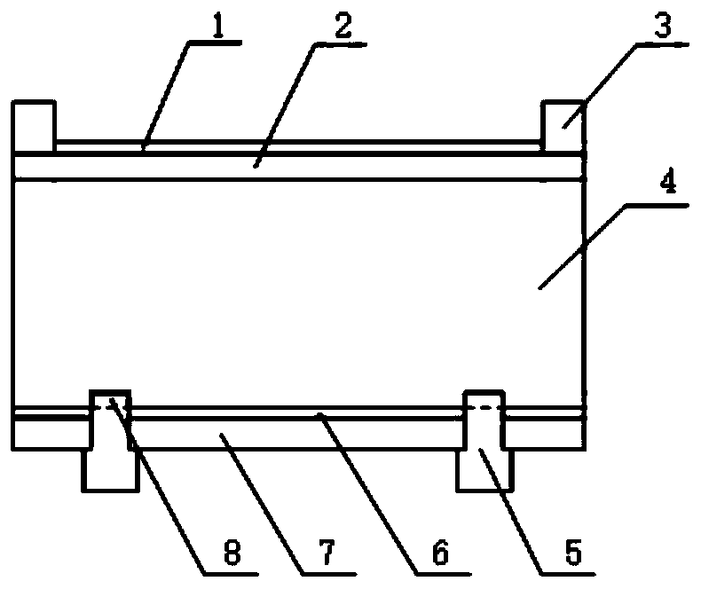
Image

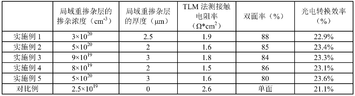
Examples
preparation example Construction
[0027] The invention provides a method for preparing a double-sided PERL solar cell, comprising the following steps:
[0028] S1. Wafer pretreatment: put P-type silicon wafer in HF / HNO 3 Washing in the mixed solution to remove the damaged layer and cutting line marks on the surface of the P-type silicon chip, and then taking it out for texturing;
[0029] S2. Silicon wafer backside treatment: the backside of the P-type silicon wafer obtained by the pretreatment in step S1 is placed in a KOH solution for polishing, and then a layer of Al is deposited on the backside of the P-type silicon wafer by PECVD. 2 o 3 layer, then the Al 2 o 3 A passivation film SiNx layer is deposited on the layer, and the Al 2 o 3The thickness of the layer is 10-20nm, and the thickness of the SiNx passivation film is 80-100nm;
[0030] S3. Front side treatment of silicon wafer: using POCl 3 As a phosphorus source, phosphorus is diffused on the front side of the P-type silicon wafer obtained in s...
Embodiment 1
[0040] The invention provides a double-sided PERL solar cell
[0041] A preparation method of a double-sided PERL solar cell comprising the steps of:
[0042] S1. Wafer pretreatment: put P-type silicon wafer in HF / HNO 3 Mixed solution (HF / HNO 3 The mixed solution consists of 40wt% HF solution and 65wt% HNO 3 Solution is configured according to the mass ratio of 1:1) to clean, remove the damaged layer and cutting line marks on the surface of the P-type silicon wafer, and then take it out for texturing;
[0043] S2. Silicon wafer backside treatment: the backside of the P-type silicon wafer obtained by step S1 pretreatment is placed in 40wt% KOH solution for polishing, and then a layer of Al is deposited on the backside of the P-type silicon wafer by PECVD method 2 o 3 layer, then in the Al 2 o 3 A passivation film SiNx layer is deposited on the layer, in which Al 2 o 3 The layer thickness is 15nm, and the passivation film SiNx layer thickness is 90nm;
[0044] S3. Front...
Embodiment 2
[0048] A preparation method of a double-sided PERL solar cell comprising the steps of:
[0049] S1. Wafer pretreatment: put P-type silicon wafer in HF / HNO 3 Mixed solution (HF / HNO 3 The mixed solution consists of 40wt% HF solution and 65wt% HNO 3 Solution is configured according to the mass ratio of 1:1) to clean, remove the damaged layer and cutting line marks on the surface of the P-type silicon wafer, and then take it out for texturing;
[0050] S2. Silicon wafer backside treatment: the backside of the P-type silicon wafer obtained by step S1 pretreatment is placed in 40wt% KOH solution for polishing, and then a layer of Al is deposited on the backside of the P-type silicon wafer by PECVD method 2 o 3 layer, then in the Al 2 o 3 A passivation film SiNx layer is deposited on the layer, in which Al 2 o 3 The layer thickness is 10nm, and the passivation film SiNx layer thickness is 80nm;
[0051] S3. Front side treatment of silicon wafer: using POCl 3 As a phosphorus ...
PUM
| Property | Measurement | Unit |
|---|---|---|
| Thickness | aaaaa | aaaaa |
| Thickness | aaaaa | aaaaa |
| Thickness | aaaaa | aaaaa |
Abstract
Description
Claims
Application Information