

Preparation method and application of organic-inorganic heterojunction
A heterojunction and heterostructure technology, which is applied in semiconductor/solid-state device manufacturing, molybdenum sulfide, electrical components, etc., can solve problems such as the inability to realize the preparation of organic-inorganic heterostructures, and achieve the elimination of contact barriers, easy operation, The effect of good contact
- Summary
- Abstract
- Description
- Claims
- Application Information
AI Technical Summary
Problems solved by technology
Method used
Image

Examples
Embodiment 1
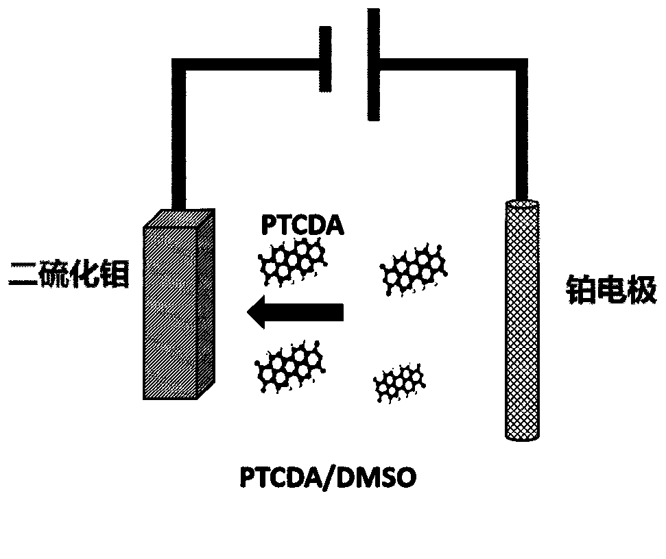
[0030] In dimethyl sulfoxide (DMSO), add 3,4,9,10-perylenetetraacid dianhydride (PTCDA), stir and dissolve completely and then precipitate, take the upper saturated solution and centrifuge at 3000r, 3min to obtain a concentration of 1g / L PTCDA / DMSO solution.
[0031] Such as figure 1 , Take the molybdenum sulfide block and clamp it with the electrode holder, immerse it in the above solution, insert a platinum electrode and a calomel reference electrode in the solution, and apply a sweep from 0V to 3V between the platinum electrode and the molybdenum sulfide electrode Voltage, scanning speed 100mV / s, PTCDA is embedded in the molybdenum sulfide layer after scanning one circle. After the reaction, the surface of the original molybdenum sulfide block was cleaned with isopropanol to obtain PTCDA / MoS 2 Organic-inorganic heterojunction.
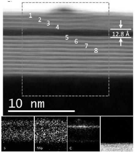
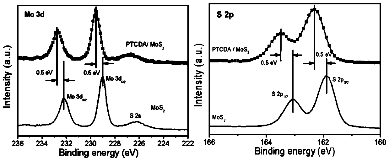
[0032] The performance characterization of organic-inorganic heterojunctions is as follows: Figure 2~4 . in, figure 2 for PTCDA / MoS 2 The ...
Embodiment 2
[0035] Adopt the method of the present invention to prepare molybdenum sulfide / PTCDA / molybdenum sulfide heterojunction, and use this organic-inorganic heterojunction as channel material to prepare molybdenum sulfide / PTCDA transistor, the preparation process is as follows Figure 5 .
[0036] (1) 275nm silicon (Si) / silicon dioxide (SiO 2 ) as the substrate, the bulk crystals were mechanically exfoliated to obtain a few-layer n-type molybdenum disulfide (MoS 2 ). The polymethyl methacrylate (PMMA) photoresist was spin-coated, the spin-coating parameter was 600r / min, 5s+4000r / min, 60s, and the baking parameter was 150°C for 10min. The photolithography and development of the electrode pattern were carried out by electron beam exposure (EBL), and the developing solution was MIBK:IPA=1:3, at room temperature for 45s. Electron beam evaporation (EBE, E-Beam Evaporation) is used to deposit 20nm Ti / 50nm Pd to obtain a contact electrode, and a back gate molybdenum sulfide field effect...
Embodiment 3
[0040] With reference to the method of Example 2, replace PTCDA with C60 and pentacene ("Pentacene"), replace molybdenum sulfide with tungsten sulfide and highly oriented pyrolytic graphite ("HOPG"), and prepare 9 kinds of organic compounds with different raw materials respectively. Inorganic heterojunction field effect transistors.
[0041] The transfer characteristic curves before and after intercalation of different organic-inorganic combined field-effect transistors (FETs) are as follows: Figure 9 , it can be seen that, in addition to WS 2 / Pentacene, it can be seen from the transfer curve that the switching ratio decreases, an obvious N doping is seen, and the current rises, that is, organic and inorganic heterostructures are realized in the field effect transistors prepared.
PUM
 Abstract
Description
Claims
Application Information