Field effect transistor and preparation method and application thereof

A technology of field-effect transistors and two-dimensional nanomaterials, applied in transistors, semiconductor/solid-state device manufacturing, semiconductor devices, etc., can solve problems affecting performance and power consumption value

Active Publication Date: 2020-07-28
THE NAT CENT FOR NANOSCI & TECH NCNST OF CHINA
View PDF12 Cites 1 Cited by
  • Summary
  • Abstract
  • Description
  • Claims
  • Application Information

AI Technical Summary

Problems solved by technology

For example, there are limitations in exposure light sources and yields in the preparation process; at the same time, as the size continues to shrink, gate leakage and channel leakage caused by quantum tunneling effects, hot carrier effects caused by short channels, and Problems such as channel carrier distribution quantum fluctuations are becoming more and more significant, seriously affecting the performance and power consumption value brought about by scaling down

Method used


Image

  • Field effect transistor and preparation method and application thereof
  • Field effect transistor and preparation method and application thereof
  • Field effect transistor and preparation method and application thereof

Examples


Embodiment 1

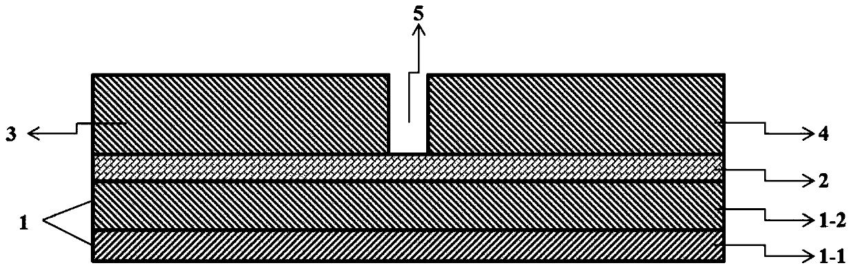
[0101] This embodiment provides a field effect transistor, the schematic cross-section of which is shown in figure 1 1 is an insulating substrate, 1-1 is silicon, 1-2 is silicon oxide, 2 is a two-dimensional nanomaterial layer, 3 is a source electrode, 4 is a drain electrode, and 5 is a conductive channel. The insulating substrate of the field effect transistor is a silicon / silicon oxide substrate, the material of the two-dimensional nano material layer is graphene, and both the source electrode and the drain electrode include a titanium adhesion metal layer and a gold electrode layer.

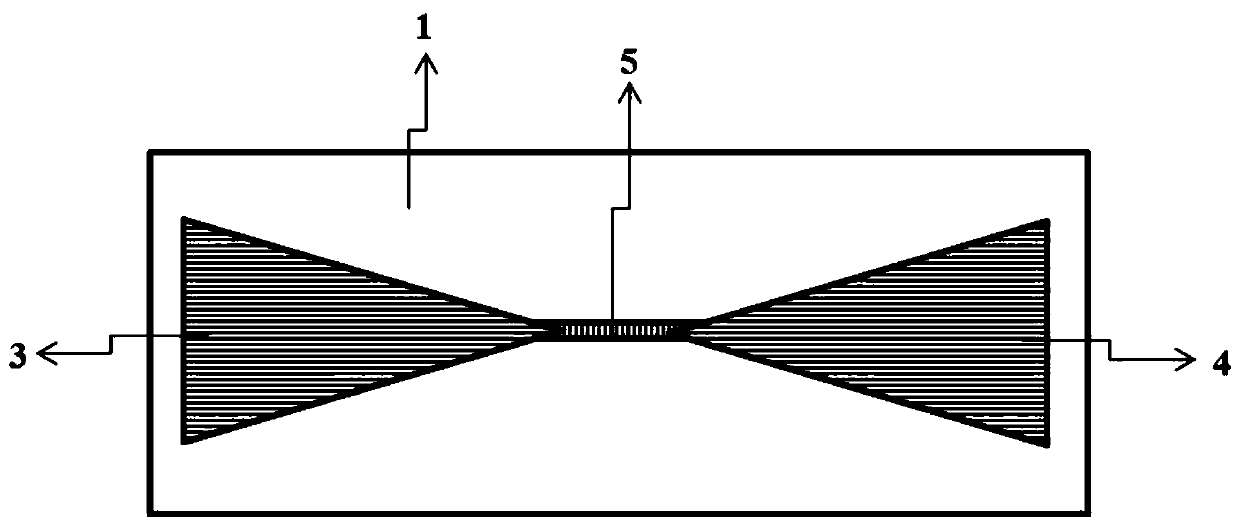
[0102] The top view of the field effect transistor is as figure 2 As shown, wherein, 1 is an insulating substrate, and the upper material is silicon oxide; 3 is a source electrode, and the upper material is gold; 4 is a drain electrode, and the upper material is gold; 5 is a conductive channel, and the upper material is graphene.

[0103] The preparation steps are as follows:

[0104] (1) C...

Embodiment 2

[0114] This embodiment provides a field effect transistor, the schematic cross-section of which is shown in Figure 6 As shown, wherein, 1 is an insulating substrate, 1-1 is silicon, 1-2 is hafnium oxide, 2 is a two-dimensional nanomaterial layer, 6 is a tunneling layer (two-dimensional boron nitride), and 3 is a source electrode, 4 is a drain electrode, and 5 is a conductive channel. The insulating substrate of the field effect transistor is a silicon / hafnium oxide substrate, the material of the two-dimensional nano material layer is molybdenum disulfide, and both the source electrode and the drain electrode include a titanium adhesion metal layer and a scandium electrode layer.

[0115] The preparation steps are as follows:

[0116] (1) Deposit a hafnium oxide insulating layer on heavily doped silicon (resistivity 0.0002Ω·cm): use atomic layer deposition equipment for deposition, the deposition thickness is 15nm, the deposition temperature is 160°C, and the source of hafniu...

Embodiment 3

[0124] This embodiment provides a field effect transistor, the schematic cross-section of which is shown in Figure 7 As shown, among them, 1 is an insulating substrate, 2 is a two-dimensional nanomaterial layer, 6 is a tunneling layer (two-dimensional boron nitride), 3 is a source electrode, 4 is a drain electrode, 5 is a conductive channel, and 7 is a top gate electrode. The insulating substrate of the field effect transistor is a sapphire substrate, the material of the two-dimensional nanomaterial layer is molybdenum disulfide, the source electrode and the drain electrode both include a titanium adhesion metal layer and a scandium electrode layer, and the top gate electrode includes a hafnium oxide insulating layer. layers and metal layers.

[0125] The preparation steps are as follows:

[0126] (1) Cut the sapphire insulating substrate into a size of 1cm×1cm, then ultrasonically clean it with acetone, isopropanol, and deionized water for 15 minutes, and dry it with nitro...


PUM

PropertyMeasurementUnit
thicknessaaaaaaaaaa
thicknessaaaaaaaaaa
thicknessaaaaaaaaaa

Abstract

The invention provides a field effect transistor and a preparation method and application thereof. The field effect transistor comprises an insulating substrate and a two-dimensional nano material layer arranged on an insulating layer of the insulating substrate, a source electrode and a drain electrode are arranged on the two-dimensional nano material layer, and the width of a conducting channelbetween the source electrode and the drain electrode is 0.5-10nm. According to the field effect transistor, the performance and the power consumption of the field effect transistor can be effectivelyimproved by controlling the conducting channel between the source electrode and the drain electrode. The conductive channel of the field effect transistor is prepared by an electric feedback method, and the electric feedback method realizes accurate control of the size of the conductive channel, so that the size of the conductive channel can be reduced to below 3nm, and the requirements of small size and high performance of a silicon-based integrated circuit technology can be met.

Description

technical field [0001] The invention belongs to the technical field of electronic materials, and in particular relates to a field effect transistor and its preparation method and application. Background technique [0002] Field effect transistor is an active device that can be controlled by free carriers. Its main components include semiconductor, source, drain and gate. The current between source and drain is controlled by gate modulation. Thus realizing the on state and the off state. In recent years, field-effect transistors, as important semiconductor devices, have been used in large-scale integrated circuits, and play an irreplaceable role in the preparation of biosensors, sensors and power control devices. [0003] One of the cores of field effect transistors lies in the channel part of the back gate modulation, and the channel of traditional field effect transistors is single crystal silicon. In the past ten years, the industry's development strategy for field effec...

Claims


Application Information

Patent Timeline
Patent Type & Authority Applications(China)
IPC IPC(8): H01L29/786H01L21/34
CPCH01L29/786H01L29/66969
Inventor 郭北斗宫建茹
Owner THE NAT CENT FOR NANOSCI & TECH NCNST OF CHINA
Why Eureka
Try Eureka