Perovskite photoelectric detector based on DNT-PH composite hole transport layer and preparation method of perovskite photoelectric detector

A technology of DNT-PH and hole transport layer, which is applied in the field of perovskite photodetectors and its preparation, can solve the problems of low mobility, short life, poor device stability, etc., and achieve simple synthesis, stability and improved life , low-cost effect

Active Publication Date: 2020-08-04
UNIV OF ELECTRONICS SCI & TECH OF CHINA
View PDF12 Cites 1 Cited by
  • Summary
  • Abstract
  • Description
  • Claims
  • Application Information

AI Technical Summary

Problems solved by technology

[0007] The object of the present invention is to: provide perovskite photodetector based on DNT-PH composite hole transport layer and preparation method thereof, to solve traditional hole transport layer material Spiro-OMeTAD low mobility, device stability is poor, life is shorter The problem

Method used


Image

  • Perovskite photoelectric detector based on DNT-PH composite hole transport layer and preparation method of perovskite photoelectric detector
  • Perovskite photoelectric detector based on DNT-PH composite hole transport layer and preparation method of perovskite photoelectric detector
  • Perovskite photoelectric detector based on DNT-PH composite hole transport layer and preparation method of perovskite photoelectric detector

Examples


Embodiment 1

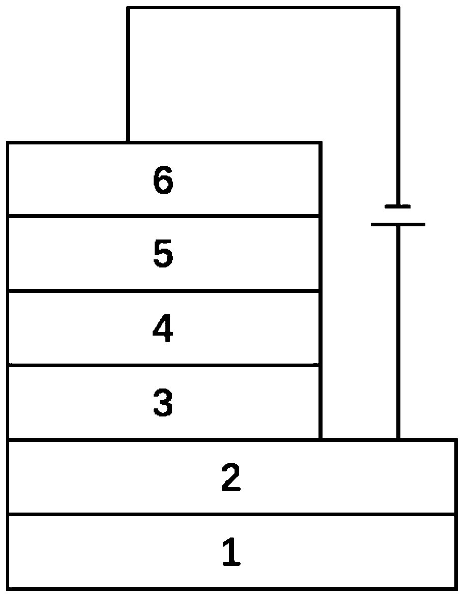
[0042] as attached Figure 1-2, clean the substrate composed of transparent substrate and conductive cathode ITO, and dry it with nitrogen after cleaning; spin-coat SnO on the surface of transparent conductive cathode ITO 2 (water dispersion, spin-coating speed is 3000rpm, spin-coating time 30s, thickness 20nm) prepare electron transport layer, and carry out thermal annealing (annealing temperature 150 ℃, annealing time 15min) of the thin film formed; Spin on the electron transport layer Coated with MAPbI 3 The precursor solution (using DMF as a solvent to form a mixed solution with a solute concentration of 500mg / mL, spin-coating speed of 4000rpm, spin-coating time of 35s, and thickness of 500nm) was used to prepare the perovskite photoactive layer. The titanite activated carbon layer was quickly dripped with chlorobenzene solution to inhibit the disordered crystallization of perovskite, and then annealed at a temperature of 110°C for 20 minutes; the surface of the perovskit...

Embodiment 2

[0044] as attached Figure 1-2 , based on Example 1, the substrate composed of transparent substrate and conductive cathode ITO is cleaned, and dried with nitrogen after cleaning; spin-coating SnO on the surface of transparent conductive cathode ITO 2 (water dispersion, spin coating speed is 3000rpm, spin coating time 30s, thickness 25nm) to prepare the electron transport layer, and carry out thermal annealing (annealing temperature 150 ℃, annealing time 15min) of the thin film formed; Spin on the electron transport layer Coated with MAPbI 3 The precursor solution (using DMF as a solvent to form a mixed solution with a solute concentration of 500mg / mL, spin-coating speed of 4500rpm, spin-coating time of 30s, and a thickness of 300nm) was used to prepare the perovskite photoactive layer. The titanite activated carbon layer was quickly dripped with chlorobenzene solution to inhibit the disordered crystallization of perovskite, and then annealed at a temperature of 115°C for 18 ...

Embodiment 3

[0046] as attached Figure 1-2 , based on Example 1, the substrate composed of the substrate and the transparent conductive cathode ITO is cleaned, and dried with nitrogen after cleaning; the surface of the transparent conductive cathode ITO is spin-coated with SnO 2 (water dispersion, spin-coating speed is 3000rpm, spin-coating time 30s, thickness 30nm) prepare electron transport layer, and carry out thermal annealing (annealing temperature 150 ℃, annealing time 15min) to the thin film formed; Spin on the electron transport layer Coated with MAPbI 3 The precursor solution (using DMF as a solvent to form a mixed solution with a solute concentration of 500mg / mL, spin-coating speed of 5000rpm, spin-coating time of 25s, and thickness of 700nm) was used to prepare the perovskite photoactive layer. The titanite activated carbon layer was quickly dripped with chlorobenzene solution to inhibit the disordered crystallization of perovskite, and then annealed at 120°C for 15 minutes; t...


PUM

PropertyMeasurementUnit
thicknessaaaaaaaaaa
thicknessaaaaaaaaaa
thicknessaaaaaaaaaa

Abstract

The invention discloses a perovskite photoelectric detector based on a DNT-PH composite hole transport layer and a preparation method thereof. The photoelectric detector is used for industrial automation, aerospace, fire early warning and other devices. The invention belongs to the technical field of photoelectric detection, and the problems that a traditional hole transport layer material Spiro-OMeTAD is low in migration rate, poor in device stability and short in service life are solved. The photoelectric detector sequentially comprises a transparent substrate, a conductive cathode, an electron transport layer, a perovskite photoactive layer, a composite hole transport layer and a metal anode from bottom to top, the composite hole transport layer is of a double-layer structure, a lower-layer film is made of Spiro-OMeTAD, and an upper-layer film is made of DNT-PH small molecules. The DNT-PH has a relatively high homo energy level; the charge transfer between the hole transport layer and the electrode can be promoted; meanwhile, the recombination of carriers is inhibited in a dark state such that the photocurrent is improved, the dark current is greatly reduced, DNT-PH covers the surface of the Spiro-OMeTAD, the corrosion of water and oxygen to the device can be effectively reduced, the stability is further enhanced, and the stability and the service life of the device are greatly improved.

Description

technical field [0001] The invention belongs to the technical field of photoelectric detection, and in particular relates to a perovskite photodetector based on a DNT-PH composite hole transport layer and a preparation method thereof. Background technique [0002] With the development of human society, mankind has entered the information age. While the Internet brings society into intelligence, automation and high speed, it also improves the efficiency, integration, multi-function, energy saving and miniaturization of various equipment. Higher requirements have been put forward in terms of globalization and environmental protection. Since it is difficult for traditional electronic equipment to meet the requirements of so many indicators at the same time, a large number of emerging multi-functional, integrated and intelligent integrated equipment have emerged as the times require. Among them, photodetectors can be used in machine vision, aerospace technology, missile tail fl...

Claims


Application Information

Patent Timeline
Patent Type & Authority Applications(China)
IPC IPC(8): H01L51/42H01L51/46H01L51/48
CPCH10K85/649H10K30/15Y02E10/549Y02P70/50
Inventor 于军胜郑丁张磊高林
Owner UNIV OF ELECTRONICS SCI & TECH OF CHINA
Why Eureka
Try Eureka