Josephson traveling wave amplifier and preparation method thereof

An amplifier and microwave technology, applied in the field of Josephson traveling wave amplifier and its preparation, can solve the problems of complex structure and difficult processing in the laboratory, and achieve the effects of simplifying the preparation steps, avoiding excessive device size and improving performance

Pending Publication Date: 2020-09-08
北京量子信息科学研究院
View PDF5 Cites 3 Cited by
  • Summary
  • Abstract
  • Description
  • Claims
  • Application Information

AI Technical Summary

Problems solved by technology

[0004] However, the existing Josephson traveling wave amplifier has a complex structure, many types of materials used, and the preparation proces

Method used


Image

  • Josephson traveling wave amplifier and preparation method thereof
  • Josephson traveling wave amplifier and preparation method thereof
  • Josephson traveling wave amplifier and preparation method thereof

Examples


Embodiment 1

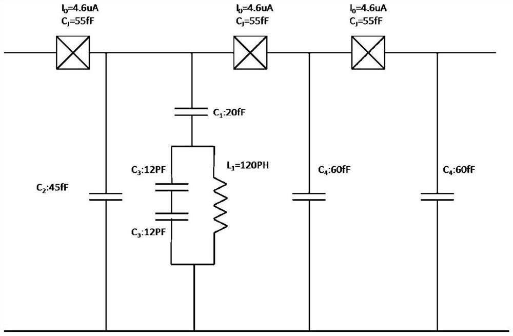
[0035] Embodiment 1 of the present application provides a Josephson traveling wave amplifier, which can meet the needs of measuring weak signals close to the quantum limit, can be applied in the measurement of qubits, simplifies the preparation process, greatly reduces the difficulty of device preparation, and can ensure The performance of the device meets the requirements.

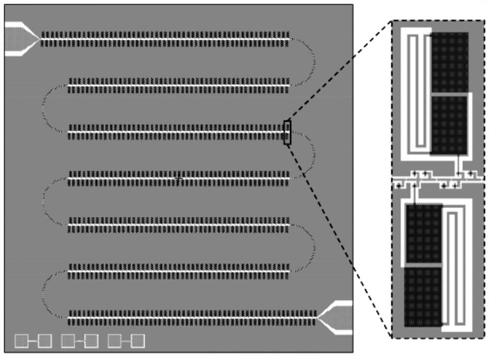
[0036] figure 1 Schematic diagram of the structure of a Josephson traveling wave amplifier. The Josephson traveling wave amplifier is a three-layer film structure, including two layers of metal layers and an intermediate dielectric layer (the dark part in the figure shows the first metal layer, the grid structure in the figure is the second metal layer, and the intermediate dielectric layer Not shown); wherein the first metal layer is made of aluminum thin film material, and the lower panel, inductor and ground plane of the capacitor are prepared by ultraviolet lithography; the second metal layer is prep...

Embodiment 2

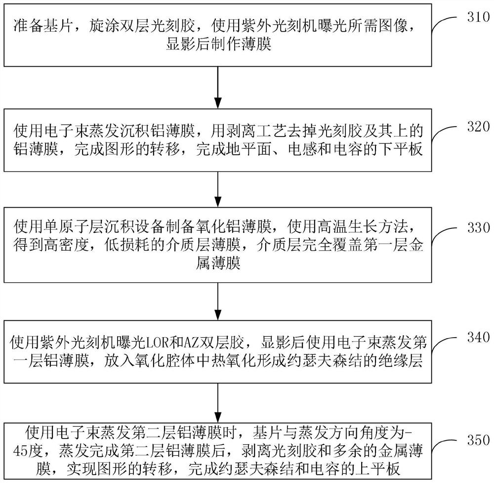
[0043] Embodiment 2 of the present application provides a method for preparing a Josephson traveling wave amplifier, such as image 3 shown, including:

[0044] Step 310, preparing the substrate, spin-coating a double-layer photoresist, exposing the required image with an ultraviolet lithography machine, and making a thin film after developing;

[0045] The devices to be used in this application include monoatomic layer deposition equipment, ultraviolet lithography machine and electron beam evaporation equipment. The devices of this application are all prepared on an undoped intrinsic silicon substrate, the substrate size is 6mm×6mm, and the substrate thickness is 0.5mm. Since this silicon substrate is not doped, the loss is very low, and the entire device The length of the transmission line is about 30mm, and the attenuation of the microwave on the transmission line can be controlled below 1dB; after preparing the substrate, spin-coat the double-layer photoresist, generally ...


PUM

PropertyMeasurementUnit
Thicknessaaaaaaaaaa
Thicknessaaaaaaaaaa
Thicknessaaaaaaaaaa

Abstract

The invention discloses a Josephson traveling wave amplifier and a preparation method thereof. The Josephson traveling wave amplifier comprises two metal layers and an intermediate dielectric layer; the first metal layer is an aluminum film, and a lower panel, an inductor and a ground plane of the capacitor are prepared through ultraviolet lithography; a second metal layer is used for preparing anupper panel of the Josephson junction and the capacitor through double-angle evaporation; the intermediate dielectric layer completely covers the first metal layer by using an aluminum oxide film grown by monoatomic layer deposition; wherein the Josephson structures form a transmission line, and two ends of the transmission line respectively form an input port and an output port of the Josephsontraveling wave amplifier; the Josephson junctions are connected with the ground through plate capacitors, and coplanar waveguide lines are adopted for connection at the bent positions of the transmission lines. By adopting the Josephson traveling wave amplifier provided by the invention, the material loss can be reduced, the preparation process is simplified, and the yield of device preparation isimproved.

Description

technical field [0001] The present application relates to the technical field of amplifier preparation, in particular to a Josephson traveling wave amplifier and a preparation method thereof. Background technique [0002] A Josephson traveling wave amplifier is a device that uses a Josephson junction as a nonlinear inductance element to achieve parametric amplification. The device is composed of superconducting circuit and Josephson structure. It has the advantages of low noise, small size, high efficiency and good stability. Its working range is generally 3-10GHz. [0003] There are many schemes for using the Josephson structure to form an amplifier. The traveling wave amplifier has the following advantages: 1. The bandwidth with a gain above 20dB can reach 3GHz. 2. Since the output and input ports are separated, no additional circulator is required to isolate the input and output signals. 3. It can be used in series to increase the gain. 4. The driving microwave and the...

Claims


Application Information

Patent Timeline
IPC IPC(8): H03F7/04
CPCH03F7/04
Inventor 薛光明于海峰金贻荣
Owner 北京量子信息科学研究院
Why Eureka
Try Eureka