Tunneling type photoelectric detector based on Van der Waals heterojunction and preparation method thereof

A photodetector and heterojunction technology, applied in circuits, electrical components, semiconductor devices, etc., to achieve large optical bandgap, high response, and improve the effect of interface contact quality

Pending Publication Date: 2020-09-18
HARBIN INST OF TECH
View PDF4 Cites 9 Cited by
  • Summary
  • Abstract
  • Description
  • Claims
  • Application Information

AI Technical Summary

Problems solved by technology

Third, although two-dimensional materials are only atomically thic...

Method used


Image

  • Tunneling type photoelectric detector based on Van der Waals heterojunction and preparation method thereof
  • Tunneling type photoelectric detector based on Van der Waals heterojunction and preparation method thereof
  • Tunneling type photoelectric detector based on Van der Waals heterojunction and preparation method thereof

Examples


Embodiment Construction

[0025] The present invention will be described in further detail below in conjunction with the accompanying drawings and embodiments. This embodiment is only a part of the embodiments of the present invention, not all of them. The protection scope of the present invention is not limited to the following examples.

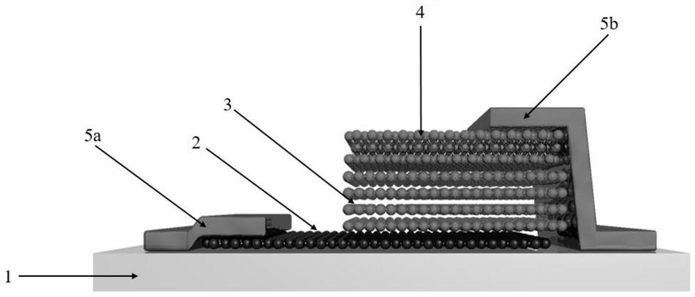
[0026] Such as figure 1 As shown, in this example, a silicon oxide wafer is used as a substrate (1), and a graphene layer (2), a hexagonal boron nitride layer (3) and a tin disulfide layer (4) form a van der Waals heterojunction to cover the substrate. The metal electrodes (5) are respectively connected to the graphene layer and the tin disulfide layer to form a photodetector.

[0027] Clean the silicon oxide wafer at 85° C. for 30 minutes with piranha lotion, and then wash it with deionized water. Then use acetone, isopropanol, ethanol and deionized water to sonicate for 10-15min in sequence. Finally, blow dry with nitrogen and set aside.

[0028] The graphene ...


PUM

PropertyMeasurementUnit
Thicknessaaaaaaaaaa
Thicknessaaaaaaaaaa
Thicknessaaaaaaaaaa

Abstract

The invention belongs to the technical field of semiconductor photoelectric detection, and particularly relates to a tunneling photoelectric detector based on a Van der Waals heterojunction and a preparation method of the tunneling photoelectric detector. A metal type two-dimensional material is used as a carrier transport layer; an insulating type two-dimensional material is used as a barrier layer and a tunneling layer; and a semiconductor type two-dimensional material is used as a photoelectric conversion material. The device structure sequentially comprises a substrate (1), a metal type two-dimensional material layer (2), an insulating type two-dimensional material tunneling layer (3), a semiconductor type two-dimensional material light absorption layer (4) and a metal electrode (5) from bottom to top. When the device works, the insulating type two-dimensional material plays a role of the barrier layer in the dark, which improves the potential barrier to prevent electron transmission, and effectively reduces the dark current of the device; under light irradiation, bias voltage is applied to enable the insulating type two-dimensional material layer to generate a tunneling effect, a conduction step of photon-generated carriers is formed, a carrier multiplication effect is generated, and the photocurrent of the device is effectively improved. The device has the characteristicsof high response rate, high detection rate, high optical switch ratio, quick response and the like.

Description

technical field [0001] The invention belongs to the field of novel material photodetectors, and mainly relates to a tunneling photodetector based on van der Waals heterojunction and a preparation method thereof. Background technique [0002] A photodetector is a device that converts an optical signal into an electrical signal based on the photoelectric effect to measure optical radiation. Due to the advantages of fast response, easy integration, high precision, small size, low power consumption and non-contact measurement, photodetectors are widely used in various fields of national economy and people's livelihood. As one of the core technologies of photodetection technology, photodetectors can quickly detect weak signals, which will affect the application range of the entire photodetection system. With the development of science and technology, although the performance of photodetectors has been significantly improved, due to the limitation of the semiconductor epitaxy pre...

Claims


Application Information

Patent Timeline
IPC IPC(8): H01L31/113H01L31/0224H01L31/032H01L31/18
CPCH01L31/1133H01L31/022408H01L31/0324H01L31/18Y02P70/50
Inventor 胡平安高峰张甲
Owner HARBIN INST OF TECH
Why Eureka
Try Eureka