Rapid expanding growth method of silicon carbide single crystal
A technology of silicon carbide single crystal and growth method, which is applied in the directions of single crystal growth, single crystal growth, crystal growth, etc., can solve the problem that the rapid diameter expansion of silicon carbide single crystal cannot be well achieved.
- Summary
- Abstract
- Description
- Claims
- Application Information
AI Technical Summary
Problems solved by technology
Method used
Image
Examples
Embodiment 1
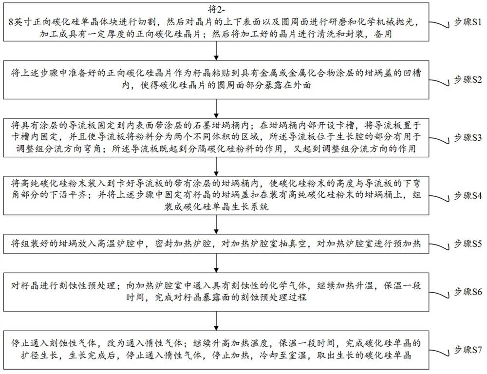
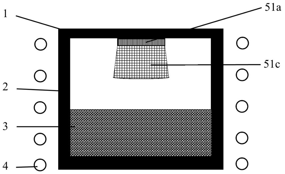
[0063] A method for rapidly expanding the diameter of a silicon carbide single crystal, the steps are as follows:
[0064] Step S1, cutting a 6-inch forward silicon carbide single crystal block, and then grinding and chemical-mechanical polishing the upper and lower surfaces and the peripheral surface of the wafer, so that the surface roughness is less than 1 nm, and processing it into a silicon carbide seed crystal with a thickness of 4 mm, Then its surface is cleaned, packaged and set aside;
[0065] Step S2, paste the forward silicon carbide wafer prepared in step S1 as a seed crystal into a groove with a tantalum carbide coating crucible cover, the depth of the groove is 1 mm, and the surface roughness of the groove pasted with the seed crystal is 5 μm, so that Part of the circumference of the silicon carbide seed crystal is exposed to the outside, ensuring that there are no gaps and air bubbles between the seed crystal and the crucible lid;
[0066] Step S3, fixing the d...
Embodiment 2
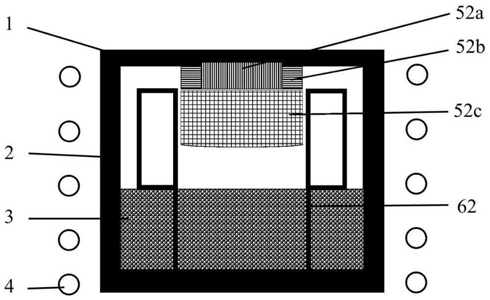
[0073] A method for rapidly expanding the diameter of a silicon carbide single crystal, the steps are as follows:
[0074] Step S1, cutting a 6-inch forward silicon carbide single crystal block, and then grinding and chemical-mechanical polishing the upper and lower surfaces and the peripheral surface of the wafer, so that the surface roughness is less than 1 nm, and processing it into a silicon carbide seed crystal with a thickness of 4 mm, Then its surface is cleaned, packaged and set aside;
[0075] Step S2, paste the forward silicon carbide wafer prepared in step S1 as a seed crystal into a groove with a tantalum carbide coating crucible cover, the depth of the groove is 1 mm, and the surface roughness of the groove pasted with the seed crystal is 5 μm, so that Part of the circumference of the silicon carbide seed crystal is exposed to the outside, ensuring that there are no gaps and air bubbles between the seed crystal and the crucible lid;
[0076] Step S3, fixing the d...
PUM
| Property | Measurement | Unit |
|---|---|---|
| surface roughness | aaaaa | aaaaa |
| diameter | aaaaa | aaaaa |
Abstract
Description
Claims
Application Information
 - R&D
- Intellectual Property
- Life Sciences
- Materials
- Tech Scout
- Unparalleled Data Quality
- Higher Quality Content
- 60% Fewer Hallucinations
Browse by: Latest US Patents, China's latest patents, Technical Efficacy Thesaurus, Application Domain, Technology Topic, Popular Technical Reports.
© 2025 PatSnap. All rights reserved.Legal|Privacy policy|Modern Slavery Act Transparency Statement|Sitemap|About US| Contact US: help@patsnap.com


