A gain-type heterojunction ultraviolet photodetector

A technology of electrical detectors and heterojunctions, applied in circuits, electrical components, semiconductor devices, etc., can solve the problems that hinder the practical application of AlGaN heterojunction photoconductive detectors, unfavorable detection of weak ultraviolet light signals, and decrease in photoelectric gain , to achieve excellent power consumption characteristics, simple preparation process, and low dark current effect

Active Publication Date: 2022-07-26
SUN YAT SEN UNIV
View PDF13 Cites 0 Cited by
  • Summary
  • Abstract
  • Description
  • Claims
  • Application Information

AI Technical Summary

Problems solved by technology

However, if there is a two-dimensional electron gas in the absence of light, the photodetector will have a high dark current, which is not conducive to detecting weak ultraviolet light signals.
In addition, even though this kind of photodetector based on the photoconductive working mechanism can have high photoelectric gain, its photoelectric gain drops seriously with the weakening of the incident light signal intensity, and it needs reinforcement
Since dark current and photoelectric gain are the key technical indicators for ultraviolet detection applications, the existence of the above problems seriously hinders the practical application of AlGaN heterojunction photoconductive detectors.

Method used


Image

  • A gain-type heterojunction ultraviolet photodetector
  • A gain-type heterojunction ultraviolet photodetector
  • A gain-type heterojunction ultraviolet photodetector

Examples


Embodiment 1

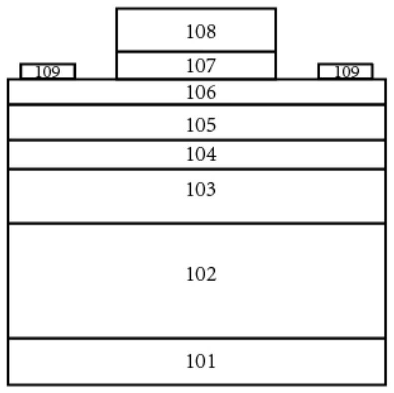
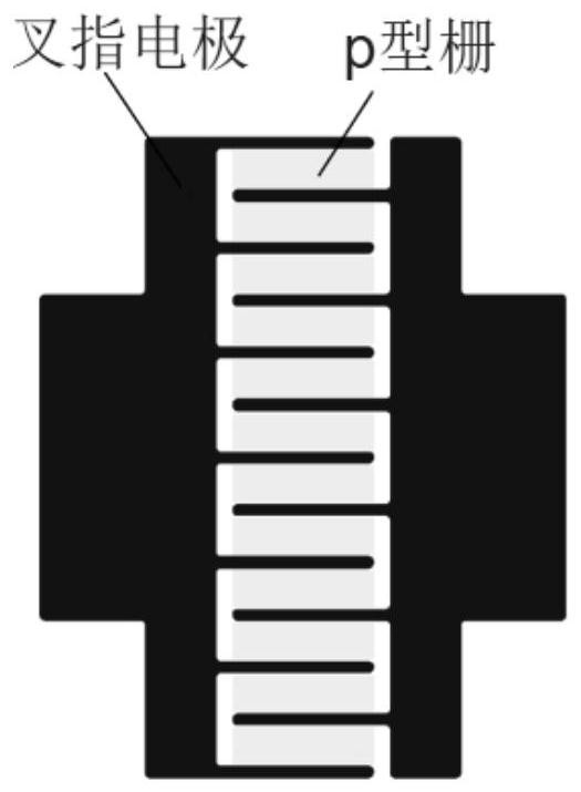
[0034] In this embodiment, an epitaxial growth method of metal organic chemical vapor deposition (MOCVD) or molecular beam epitaxy (MBE) is used to grow a gain type AlGaN heterojunction ultraviolet photodetector, which sequentially includes a c-plane sapphire substrate (201), a 20nm A low-temperature AlN nucleation layer (202) with a thickness of 500 nm, a high-temperature unintentionally doped AlN transition layer (203) with a thickness of 500 nm, and an Al and Ga alloy composition graded Al with a thickness of 100 nm x Ga 1-x N (x=0.7-0.4) layer (204), 200 nm thick unintentionally doped Al 0.4 Ga 0.6 N-layer (205), 20 nm thick unintentionally doped Al 0.6 Ga 0.4 N-layer (206), 30 nm thick unintentionally doped Al 0.4 Ga 0.6 N layer (207), 60nm thick acceptor Mg doped Al 0.43 Ga 0.57 N layer (208), the hole concentration in the layer is 3×10 18 cm -3 , and inadvertently doped Al alloys made by etching, evaporation, etc. 0.6 Ga 0.4 An interdigitated ohmic contact el...

Embodiment 2

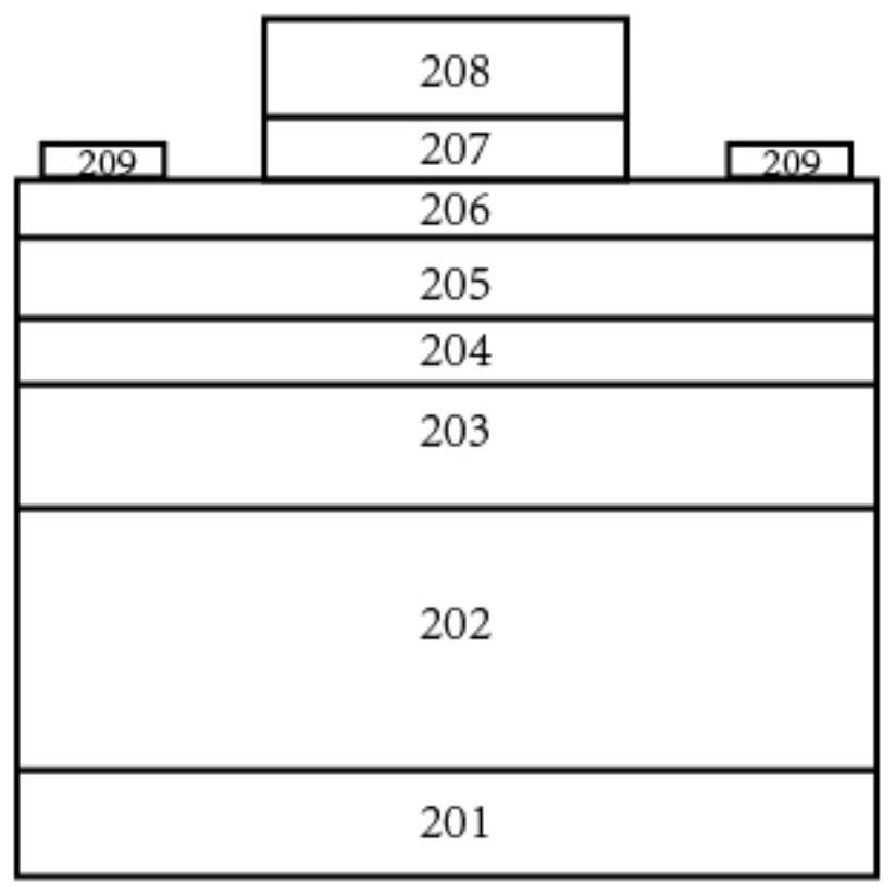
[0037] In this embodiment, a gain-type AlGaN heterojunction ultraviolet photodetector is grown by an epitaxial growth method of metal organic chemical vapor deposition (MOCVD) or molecular beam epitaxy (MBE), which sequentially includes a c-plane sapphire substrate (301), a thickness of 25 nm A low-temperature GaN nucleation layer (302), a high-temperature unintentionally doped GaN transition layer (303) with a thickness of 3 μm, a transition GaN layer with a thickness of 0 nm (that is, this layer may not be provided in this embodiment), a 1 μm-thick Unintentionally doped GaN layer (305), 25 nm thick unintentionally doped Al 0.26 Ga 0.74 N layer (306), 30nm thick unintentionally doped GaN layer (307), 60nm thick acceptor Mg-doped GaN layer (308), the hole concentration in the layers is 2 × 10 18 cm-3, and inadvertently doped Al alloys made by etching, evaporation, etc. 0.26 Ga 0.74 An interdigitated ohmic contact electrode (309) formed of a Ti / Al / Ni / Au metal layer alloy on ...


PUM

PropertyMeasurementUnit
thicknessaaaaaaaaaa
thicknessaaaaaaaaaa
thicknessaaaaaaaaaa

Abstract

The invention discloses a gain-type heterojunction ultraviolet photodetector, comprising a substrate and an epitaxial layer grown on the substrate; the epitaxial layer sequentially includes a nucleation layer, an unintentional Al doping layer from bottom to top k Ga 1‑k N buffer layer, Al x Ga 1‑x N composition transition layer, unintentional doping of Al y Ga 1‑y N layer, unintentionally doped Al z Ga 1‑z N layer, unintentionally doped Al y Ga 1‑y N layer, acceptor doped Al m Ga 1‑m N layers and distributed in unintentionally doped Al z Ga 1‑z An interdigitated contact electrode on the N layer, where the starting value of the Al composition x≤k, and the ending value is y; y<z. Al doping by acceptor m Ga 1‑m N layer to deplete unintentionally doped Al y Ga 1‑y The N layer and the top of it are unintentionally doped with Al z Ga 1‑z The two-dimensional electron gas at the interface of the N-layer heterojunction has the advantages of high light-dark rejection ratio, high photoelectric gain and fast response speed.

Description

technical field [0001] The invention relates to the technical field of group III nitride semiconductor ultraviolet photodetectors, in particular to a gain-type heterojunction ultraviolet photodetector. Background technique [0002] UV detection has a wide range of applications in both military and civilian fields, such as chemical and biological analysis (detection of ozone, pollutants and most organic compounds UV absorption lines), flame detection (including fire alarm, missile warning or combustion monitoring), security Optical communication (inter-satellite optical communication with wavelengths less than 280nm), transmitter calibration (instrumentation, UV lithography) and astronomical research, etc. At present, commercial UV detectors are mainly photomultiplier tubes (PMTs) based on vacuum electron technology and solid-state photodetectors based on mature semiconductor material Si. Photomultiplier tube detectors need to work at higher voltages (generally around 1000V)...

Claims


Application Information

Patent Timeline
Patent Type & Authority Patents(China)
IPC IPC(8): H01L31/0304H01L31/112
CPCH01L31/03048H01L31/1129
Inventor 江灏宋志远邱新嘉
Owner SUN YAT SEN UNIV
Why Eureka
Try Eureka