
A Lossless Rapid Separation Method of Single Crystal Diamond and Substrate

A single crystal diamond and separation method technology, which is applied in the field of lossless and fast separation of single crystal diamond and substrate, can solve the problems of high price, long growth cycle, loss of diamond, etc., shorten the corrosion cycle, improve separation efficiency, and save resources Effect

Active Publication Date: 2021-10-26
富山居超钻半导体科技(山东)有限公司
View PDF8 Cites 0 Cited by
  • Summary
  • Abstract
  • Description
  • Claims
  • Application Information

AI Technical Summary

Problems solved by technology

Nowadays, CVD technology is mainly used to produce diamond substrates. However, the problems of long growth cycle and high price of diamond materials still need to be solved urgently.
[0003] At present, most of the diamonds are grown by microwave plasma vapor deposition (MPCVD) technology. Although high-quality diamonds can be prepared, the growth cycle is relatively long.
Moreover, the laser cutting method used when separating the epitaxial layer will lose a part of the diamond, and the larger the size of the diamond sheet, the more loss; 2 Taking a diamond substrate as an example, laser cutting will consume a thickness of 480 μm of the substrate

Method used


Image

  • A Lossless Rapid Separation Method of Single Crystal Diamond and Substrate
  • A Lossless Rapid Separation Method of Single Crystal Diamond and Substrate
  • A Lossless Rapid Separation Method of Single Crystal Diamond and Substrate

Examples


Embodiment 1

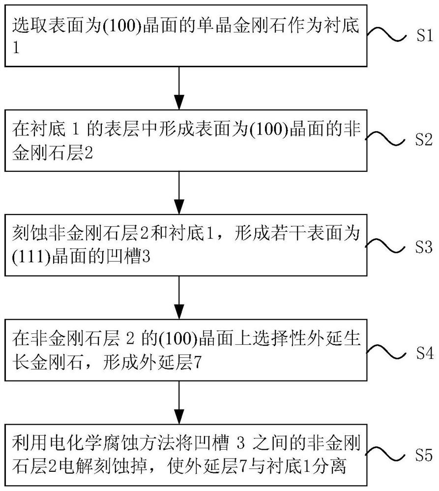
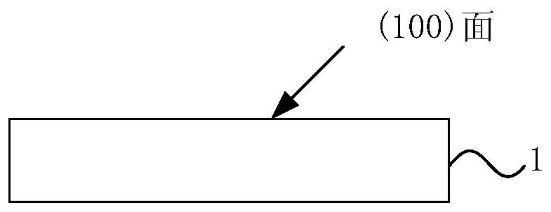
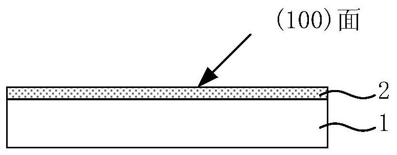
[0034] See figure 1 and Figure 2, figure 1 A schematic flow chart of a lossless and fast separation method for single crystal diamond and substrate provided by an embodiment of the present invention, Figure 2a-Figure 2h It is a process schematic diagram of a lossless and rapid separation method for single crystal diamond and a substrate provided by an embodiment of the present invention. The separation method comprises the steps of:

[0035] S1. Select the single crystal diamond whose surface is the (100) crystal plane as the substrate 1, please refer to Figure 2a .

[0036] Specifically, a single crystal diamond sheet whose surface is a (100) crystal plane synthesized by High Temperature and High Pressure (HTHP) is selected as the substrate 1 . In this embodiment, as long as the upper surface of the single crystal diamond sheet is a (100) crystal plane, there is no restriction on the side and lower surfaces of the single crystal diamond sheet, and its side and lower sur...

Embodiment 2

[0061] On the basis of Embodiment 1, this embodiment will illustrate the lossless separation method by taking the substrate 1 with a separation groove depth of 10 μm and the epitaxial layer 7 with 500 μm as an example.

[0062] Please combine figure 1 and Figure 2a-Figure 2h , the lossless separation method comprises steps:

[0063] S1. A single crystal diamond whose surface is a (100) crystal plane is selected as the substrate 1 .

[0064] S2. Forming a non-diamond layer 2 with a (100) crystal plane on the surface of the substrate 1 .

[0065] S3. Etching the non-diamond layer 2 and the substrate 1 to form several grooves 3 whose surfaces are (111) crystal planes.

[0066] Spin-coat photoresist 4 on the surface of non-diamond layer 2, and make window pattern 5 on the photoresist by contact photolithography; then prepare a layer on the surface of photoresist 4 and non-diamond layer 2 by metal evaporation 300nm thick nickel metal, the metal on the photoresist is peeled off...

Embodiment 3

[0073] On the basis of Embodiment 1, this embodiment will illustrate the lossless separation method by taking the substrate 1 with a separation groove depth of 15 μm and the epitaxial layer 7 with 1000 μm as an example.

[0074] Please combine figure 1 and Figure 2a-Figure 2h , the lossless separation method comprises steps:

[0075] S1. A single crystal diamond whose surface is a (100) crystal plane is selected as the substrate 1 .

[0076] S2. Forming a non-diamond layer 2 with a (100) crystal plane on the surface of the substrate 1 .

[0077] S3. Etching the non-diamond layer 2 and the substrate 1 to form several grooves 3 whose surfaces are (111) crystal planes.

[0078] Spin-coat photoresist 4 on the surface of non-diamond layer 2, and make window pattern 5 on the photoresist by contact photolithography; then prepare a layer on the surface of photoresist 4 and non-diamond layer 2 by metal evaporation 300nm thick nickel metal, the metal on the photoresist is peeled of...


PUM

PropertyMeasurementUnit
thicknessaaaaaaaaaa
depthaaaaaaaaaa
thicknessaaaaaaaaaa

Abstract

The invention relates to a method for fast separation of single crystal diamond and a substrate without loss, comprising the steps of: S1, selecting a single crystal diamond whose surface is a (100) crystal plane as a substrate; S2, forming a surface in the surface layer of the substrate Be the non-diamond layer of (100) crystal plane; S3, etch described non-diamond layer and described substrate, form the groove that some surfaces are (111) crystal plane; S4, in (100) of described non-diamond layer ) selective epitaxial growth of diamond on the crystal surface to form an epitaxial layer; S5, using an electrochemical etching method to electrolytically etch the non-diamond layer between the grooves to separate the epitaxial layer from the substrate . The separation method pre-etches (111) crystal plane grooves on the diamond substrate, then performs (100) crystal plane selective epitaxy, and then uses electrochemical etching to etch away the non-diamond layer between adjacent grooves, To achieve the purpose of separating the substrate and the epitaxial layer, the separation speed is greatly improved due to the small etching depth.

Description

technical field [0001] The invention belongs to the technical field of microelectronics, and in particular relates to a lossless and rapid separation method for single crystal diamond and a substrate. Background technique [0002] As a wide bandgap semiconductor material, diamond has many unique physical properties, such as high thermal conductivity, high hardness, and high carrier mobility. It is an ideal material for making power electronic devices and detectors, and can be used for high temperature, high power and strong In harsh environments with radiation. Nowadays, CVD technology is mainly used to produce diamond substrates, but the problems of long growth cycle and high price of diamond materials still need to be solved urgently. [0003] At present, most diamonds are grown by microwave plasma vapor deposition (MPCVD) technology. Although high-quality diamonds can be produced, the growth cycle is relatively long. Moreover, the laser cutting method used when separati...

Claims


Application Information

Patent Timeline
Patent Type & Authority Patents(China)
IPC IPC(8): C25F3/12C25F3/14C23C14/48C23C14/06C23C14/24C23C14/18C30B25/20C30B29/04
CPCC23C14/0605C23C14/18C23C14/24C23C14/48C25F3/12C25F3/14C30B25/20C30B29/04
Inventor 任泽阳邢雨菲张金风张进成何琦苏凯郝跃
Owner 富山居超钻半导体科技(山东)有限公司
Learn More