
Preparation process suitable for superconducting detector glass window

A technology of superconducting detector and preparation process, applied in the field of superconducting electronics, can solve the problems of detector pattern damage, extremely thin glass window being fragile, unable to withstand high back helium gas pressure, etc., to reduce noise and improve performance effect

Pending Publication Date: 2020-12-25
SHANGHAI TECH UNIV
View PDF0 Cites 1 Cited by
  • Summary
  • Abstract
  • Description
  • Claims
  • Application Information

AI Technical Summary

Problems solved by technology

[0006] The technical problem to be solved by the present invention is to solve the problem that the extremely thin glass window cannot withstand the high back helium pressure when preparing the superconducting detector glass window for cosmic microwave background radiation detection; The problem that the prepared detector pattern is damaged; solve the problem that the extremely thin glass window is fragile during the whole process, such as the separation of the chip and the glass window wafer, removal of photoresist residue, chip cleaning, and chip drying

Method used


Image

  • Preparation process suitable for superconducting detector glass window
  • Preparation process suitable for superconducting detector glass window
  • Preparation process suitable for superconducting detector glass window

Examples


Embodiment

[0034]A preparation process suitable for glass windows of superconducting detectors includes the following steps:

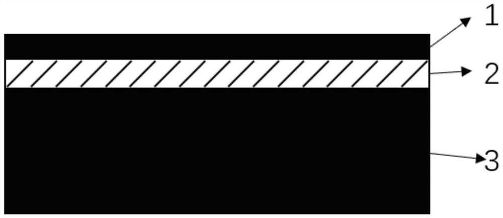
[0035]Step 1: Prepare a glass window wafer, which in turn includes a glass window layer 1, a silicon dioxide stop layer 2 and a silicon layer 3 made of silicon or silicon nitride, such asfigure 1 Shown

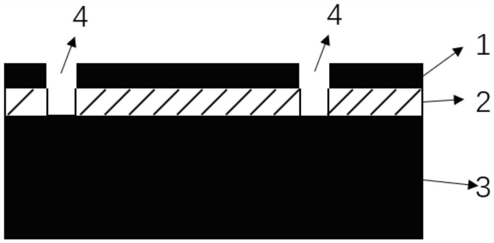
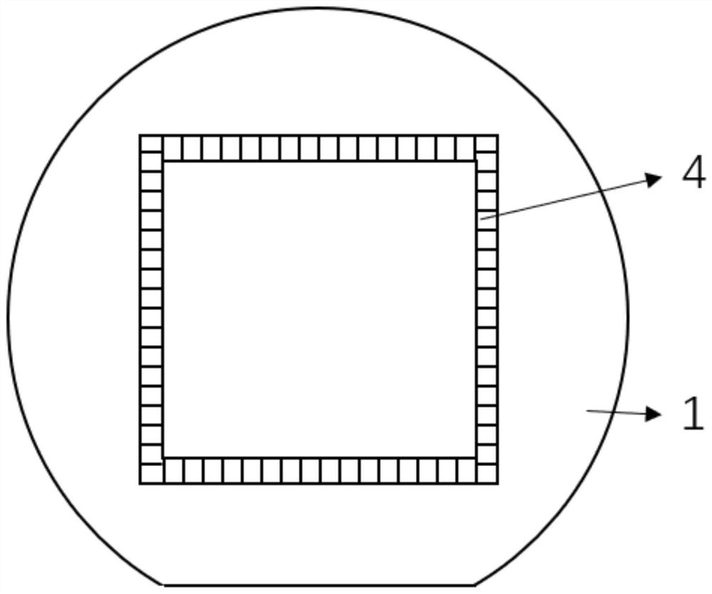
[0036]Step 2: Use a photolithography process to prepare the chip boundary cutting groove pattern on the glass window layer 1, and use a fluorine-based gas to etch the chip boundary cutting groove 4 until the silicon or silicon nitride in the chip boundary cutting groove 4 and the second The silicon oxide stop layer is completely etched, such asfigure 2 ,3Shown

[0037]Step 3: Use the organic solvent acetone to dissolve the paraffin to prepare an adhesive; bond the glass window layer 1 side of the glass window wafer to a piece of carrier wafer 5 with the prepared adhesive, such asFigure 4 As shown; when the glass window layer 1 and the carrier wafer 5 are bonded, it must be ensu...


PUM

PropertyMeasurementUnit
thicknessaaaaaaaaaa
thicknessaaaaaaaaaa
thicknessaaaaaaaaaa

Abstract

The invention discloses a preparation process suitable for a superconducting detector glass window, which is characterized by comprising the following steps of cutting a chip boundary cutting groove Ion one side of the glass window of a glass window wafer, and completely etching silicon or silicon nitride and a cut-off layer in the chip boundary cutting groove I, bonding one side of a glass window of the glass window wafer with the bearing wafer, etching a glass window on one side of the silicon layer of the bonded wafer, and etching a chip boundary cutting groove II at a position corresponding to the chip boundary cutting groove I to expose the cut-off layer, cleaning the residual photoresist by adopting oxygen plasma, separating the glass window wafer and the bearing wafer by using an organic solvent, and separating the glass window-containing chip from the glass window wafer. By adopting the preparation scheme of the superconducting detector glass window suitable for universe microwave background radiation detection provided by the invention, the success rate of preparing the glass window containing the detector pattern can be improved to 100%, and the success rate of separating the chip containing the glass window from the glass window wafer also reaches 100%.

Description

Technical field[0001]The invention relates to a preparation process of a superconducting detector glass window suitable for the detection of cosmic microwave background radiation, and belongs to the technical field of superconductivity electronics.Background technique[0002]Superconductivity electronics is an interdisciplinary subject that combines superconducting physics and electronic technology. It is based on superconducting micro-theories and various quantum effects. It uses Josephson junctions and superconducting planar micro-nano structures as the main structural units to form Passive devices, microwave active devices, sensors / detectors and other superconducting electronic devices and circuits have unparalleled advantages over traditional semiconductor devices and circuits in terms of noise, speed, power consumption, and bandwidth. Fields such as limited sensitivity detection, quantum information processing, quantum metrology, high-performance computing, and cutting-edge basic...

Claims


Application Information

Patent Timeline
Patent Type & Authority Applications(China)
IPC IPC(8): B81C1/00B81B7/00
CPCB81B7/0077B81C1/00333B81B2201/02Y02P70/50
Inventor 宋艳汝杨瑾屏刘志
Owner SHANGHAI TECH UNIV
Learn More