High-color-saturation silicon-based OLED micro display device and preparation method thereof

A micro-display and saturation technology, which is applied in semiconductor/solid-state device manufacturing, electric solid-state devices, semiconductor devices, etc., can solve the problems of poor display effect and low color saturation of devices, and achieve reduced production costs, wide process window, Realize the effect of refined production

Pending Publication Date: 2021-01-08
YUNNAN NORTH OLIGHTEK OPTO ELECTRONICS TECH
View PDF0 Cites 4 Cited by
  • Summary
  • Abstract
  • Description
  • Claims
  • Application Information

AI Technical Summary

Problems solved by technology

[0007] Aiming at the shortcomings of low color saturation and poor display effect of the current silicon-based OLED microdisplay, the present invention proposes a silicon-based OLED microdisplay based on quantum dots and high-efficiency blue light and its preparation method

Method used


Image

  • High-color-saturation silicon-based OLED micro display device and preparation method thereof
  • High-color-saturation silicon-based OLED micro display device and preparation method thereof

Examples


Embodiment 1

[0028] Embodiment 1: the preparation method of silicon-based OLED microdisplay, comprises the following steps:

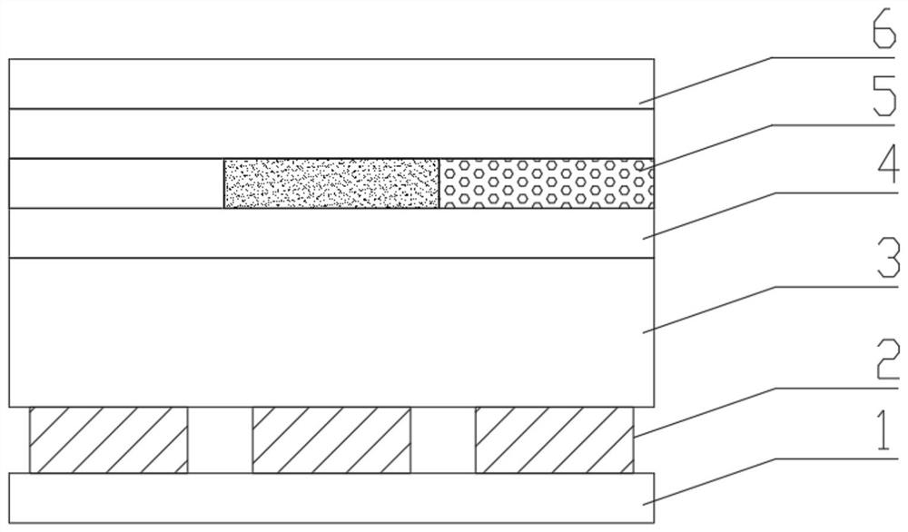
[0029] In the first step, on the 8-inch 0.13µm silicon-based drive circuit, the three-layer anode Cr / Al / AlN is prepared by PVD methods such as electron beam evaporation, thermal evaporation, and ion beam-assisted deposition. The total thickness of the three-layer anode is controlled at 20 ~100nm, among which, the thickness of metal Cr is 5~40nm, the thickness of metal Al is 20~50nm, and the thickness of AlN is 1~3nm.

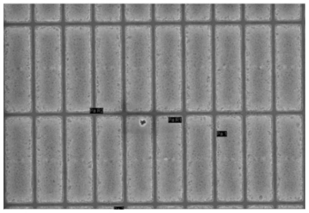
[0030] In the second step, the anode pixels are prepared by dry etching process, the pixel size is 3.3µm×9.9µm, and the pixel pitch is 0.8µm.

[0031] The third step is to prepare hole injection layer, hole transport layer, light emitting layer, electron transport layer, electron injection layer, translucent cathode Mg:Ag and anti-reflection layer with high refractive index by evaporation on the anode pixel points by masking. layer material. Wherein...

Embodiment 2

[0035] Embodiment 2: the preparation method of silicon-based OLED microdisplay, comprises the following steps:

[0036] In the first step, on a 12-inch 0.11µm silicon-based drive circuit, two layers of anode Al / AlN are prepared by PVD methods such as electron beam evaporation, thermal evaporation, and ion beam assisted deposition. The thickness of the two layers of anode is controlled in the range of 20~100nm. Among them, the thickness of metal Al is 20~50nm, and the thickness of AlN is 1~3nm;

[0037] In the second step, the anode pixels are prepared by dry etching process, the pixel size is 5µm×15µm, and the pixel pitch is 1µm.

[0038] The third step is to prepare hole injection layer, hole transport layer, light emitting layer, electron transport layer, electron injection layer, translucent cathode Mg:Ag and anti-reflection layer with high refractive index by evaporation on the anode pixel points by mask method. layer material.

[0039] The fourth step is to prepare red,...


PUM

PropertyMeasurementUnit
widthaaaaaaaaaa
thicknessaaaaaaaaaa
thicknessaaaaaaaaaa

Abstract

The invention relates to the technical field of organic light-emitting diode manufacturing, particularly to a silicon-based OLED micro display device and a preparation method thereof. The display device is composed of a silicon-based CMOS drive circuit substrate, a top light-emitting multilayer composite anode, a blue light organic light-emitting layer, an antireflection layer, a quantum dot colorfilter layer, an inorganic or polymer composite film sealing layer and a glass cover plate. In the preparation of the display device, a dry etching process is used for preparing composite anode pixelpoints, and a doping mode is used for realizing the preparation of a blue light organic light-emitting layer. The display device has the characteristic of low optical loss.

Description

technical field [0001] The invention relates to the technical field of organic light-emitting diode manufacturing, in particular to a silicon-based OLED microdisplay and a preparation method thereof. Background technique [0002] Silicon-based OLED microdisplays are an important branch of organic display technology. Silicon-based OLED microdisplay has self-illumination, thin thickness, light weight, impact resistance, vibration resistance, large viewing angle, short response time, good high and low temperature characteristics, high luminous efficiency, low power consumption, high integration, small size, and easy to carry and other excellent characteristics. It has important application prospects in the fields of military, aerospace and personal consumer electronics. With changes in the national military security situation and individual consumer electronics needs, the market demand for high-performance microdisplays is becoming more and more urgent. [0003] At present, ...

Claims


Application Information

Patent Timeline
Patent Type & Authority Applications(China)
IPC IPC(8): H01L27/32H01L51/52H01L51/56
CPCH10K59/38H10K59/12H10K50/81H10K59/1201H10K71/00
Inventor 王光华陈雪梅杨丽丽高思博段登辉季华夏
Owner YUNNAN NORTH OLIGHTEK OPTO ELECTRONICS TECH
Why Eureka
Try Eureka