Film ultraviolet detector and preparation method thereof

A UV detector and thin film technology, applied in semiconductor devices, final product manufacturing, sustainable manufacturing/processing, etc., can solve the problems of narrow band gap and limited application, and achieve the effect of mild conditions, simple steps and large area

Active Publication Date: 2021-03-12
CHANGCHUN INST OF OPTICS FINE MECHANICS & PHYSICS CHINESE ACAD OF SCI
View PDF9 Cites 0 Cited by
  • Summary
  • Abstract
  • Description
  • Claims
  • Application Information

AI Technical Summary

Problems solved by technology

Due to the common BaTiO 3 The bandgap is too narrow, the corresponding optical absorption edge is 361nm, it is not suitable as a UV detector in the UVB band, and it has no spectral selectivity for UVB, which also limits its application in the UVB band photodetector

Method used


Image

  • Film ultraviolet detector and preparation method thereof
  • Film ultraviolet detector and preparation method thereof
  • Film ultraviolet detector and preparation method thereof

Examples


Embodiment 1

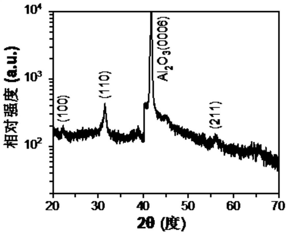
[0052] Figure 2-6 It is a kind of BaTiO provided by the present invention 3 BaTiO in Thin Film Ultraviolet Detector and Preparation Method Embodiment 1 3 Thin film test data.

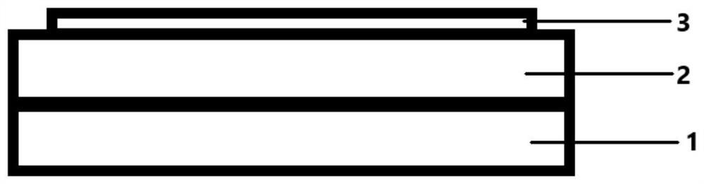
[0053] Put the cleaned sapphire substrate into the magnetron sputtering growth chamber, adjust the growth temperature to 500°C, and the pressure to 1×10 -1 Pa. Use BaTiO with an elemental ratio of Ba and Ti of 1:1 3 Target material, sputtering RF power is 60W, grows for 2h, turns off the RF, lowers the substrate temperature to room temperature, and obtains BaTiO 3 film.

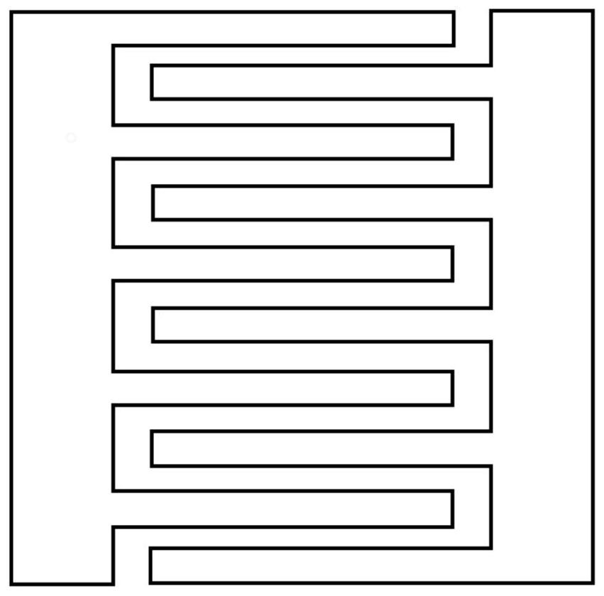
[0054] In BaTiO 3 Use negative photolithography to form 20 pairs of interdigitated electrode masks with a spacing of 5 μm and a length of 500 μm on the thin film material: put the obtained sample into a small coating machine, and under the condition of a pressure of 6 Pa and a current of 9 mA, sputter Then, the colloidal mask was removed by ultrasound for 3 minutes to form a platinum interdigitated electrode layer, and BaTiO wi...

Embodiment 2

[0061] Figure 7-10 It is a kind of BaTiO provided by the present invention 3 BaTiO in Thin Film Ultraviolet Detector and Preparation Method Embodiment 2 3 Thin film test data.

[0062] Put the cleaned sapphire substrate into the magnetron sputtering growth chamber, adjust the growth temperature to 20°C, and the pressure to 1×10 -2 Pa. Use BaTiO with an elemental ratio of Ba and Ti of 1:1 3 For the target material, the sputtering RF power is 40W, grow for 1h, turn off the RF, lower the substrate temperature to room temperature, and obtain BaTiO 3 film.

[0063] In BaTiO 3 On the film material, 20 pairs of interdigitated electrode masks with a pitch of 5 μm and a length of 500 μm were formed using negative resist lithography. The obtained sample was put into a small coating machine, and metal platinum was sputtered under the condition of a pressure of 6 Pa and a current of 9 mA. Then the colloidal mask was removed by ultrasonication for 3min to obtain BaTiO with MSM str...

Embodiment 3

[0070] Figure 11-14 It is a kind of BaTiO provided by the present invention 3 BaTiO in Thin Film Ultraviolet Detector and Preparation Method Embodiment 3 3 Thin film test data.

[0071] Put the cleaned sapphire substrate into the magnetron sputtering growth chamber, adjust the growth temperature to 500°C, and the pressure to 1×10Pa. Use BaTiO with an elemental ratio of Ba and Ti of 1:1 3 For the target material, the sputtering RF power is 180W, grow for 2h, turn off the RF, lower the substrate temperature to room temperature, and obtain BaTiO 3 film.

[0072] In BaTiO 3 On the film material, 20 pairs of interdigitated electrode masks with a pitch of 5 μm and a length of 500 μm were formed using negative resist lithography. The obtained sample was put into a small coating machine, and metal platinum was sputtered under the condition of a pressure of 6 Pa and a current of 9 mA. Then the colloidal mask was removed by ultrasonication for 3min to obtain BaTiO with MSM struc...


PUM

PropertyMeasurementUnit
particle sizeaaaaaaaaaa
thicknessaaaaaaaaaa
thicknessaaaaaaaaaa

Abstract

The invention provides a BaTiO3 thin film ultraviolet detector and a preparation method thereof, and particularly relates to a BaTiO3 thin film with a forbidden band width of 3.9-4.4 eV. The detectorcomprises a substrate, a BaTiO3 film growing on the upper surface of the substrate, and an interdigital electrode layer compounded on the BaTiO3 film, the forbidden band width of the BaTiO3 thin filmis 3.9 to 4.4 eV; the grain size of the BaTiO3 thin film ranges from 0.01 nm to 30 nm; the thickness of the BaTiO3 thin film ranges from 50 nm to 500 nm; and the light absorption cut-off edge of the BaTiO3 thin film is 280 to 320 nm. The BaTiO3 film prepared by the method has the characteristics of small grain size, wide energy gap, absorption cutoff edge of 280-320 nm and the like, so that the detection wavelength corresponding to a BaTiO3 ultraviolet detector is 280-320 nm, the BaTiO3 film is an excellent UVB photoelectric detection material, detection of BaTiO3 to the UVB waveband is realized, and application of the BaTiO3 film in the field of UVB ultraviolet detectors is broadened.

Description

technical field [0001] The invention relates to the field of semiconductor material growth, in particular to a BaTiO 3 Thin film ultraviolet detector and its preparation method. Background technique [0002] Sunlight is one of the basic energy sources for the survival and development of human society. Although ultraviolet (10-400nm) radiation is only a small proportion of solar radiation, it has an important impact on the life of human beings. Ultraviolet light can be divided according to wavelength: ultraviolet A (UVA) with a wavelength of 320-400nm; ultraviolet B (UVB) with a wavelength of 280-320nm; ultraviolet C (UVC) with a wavelength of 100-280nm. Among them, ultraviolet B (UVB) radiation is closely related to human health. On the one hand, a moderate amount of UVB radiation is beneficial to the formation of vitamin D in humans, which can reduce the risk of cancer. On the other hand, too much UVB radiation can suppress the immune system, cause cataracts and lead to ...

Claims


Application Information

Patent Timeline
Patent Type & Authority Applications(China)
IPC IPC(8): H01L31/032H01L31/108H01L31/18
CPCH01L31/032H01L31/1085H01L31/18Y02P70/50
Inventor 刘可为韩无双申德振陈星张振中李炳辉
Owner CHANGCHUN INST OF OPTICS FINE MECHANICS & PHYSICS CHINESE ACAD OF SCI
Why Eureka
Try Eureka