Lead salt film structure for infrared photoelectricity and preparation method thereof

A lead-salt and thin-film technology, used in circuits, electrical components, final product manufacturing, etc., to improve the specific detection rate, reduce low-frequency noise, and achieve high uniformity

Active Publication Date: 2021-03-19
CHONGQING INST OF GREEN & INTELLIGENT TECH CHINESE ACADEMY OF SCI
View PDF8 Cites 3 Cited by
  • Summary
  • Abstract
  • Description
  • Claims
  • Application Information

AI Technical Summary

Problems solved by technology

According to previous surveys, no relevant literature has been found to disclose the preparation of lead salt thin films by combining physical vapor deposition and chemical water bath method

Method used


Image

  • Lead salt film structure for infrared photoelectricity and preparation method thereof
  • Lead salt film structure for infrared photoelectricity and preparation method thereof
  • Lead salt film structure for infrared photoelectricity and preparation method thereof

Examples


Embodiment 1

[0045] Embodiment 1 composite structure lead salt film structure

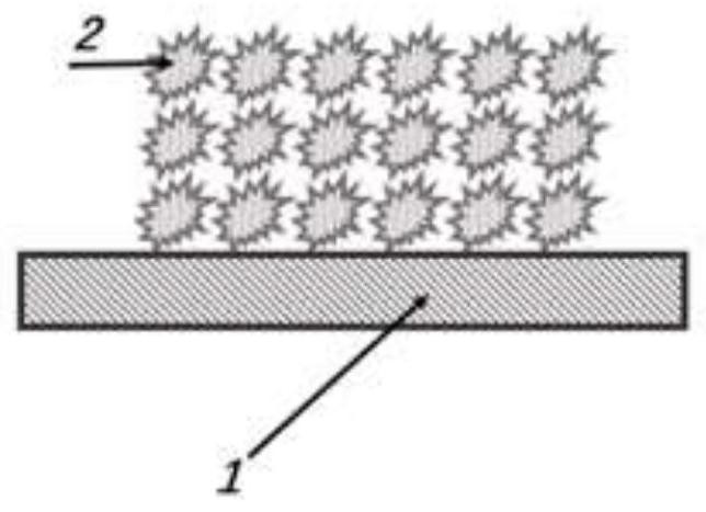
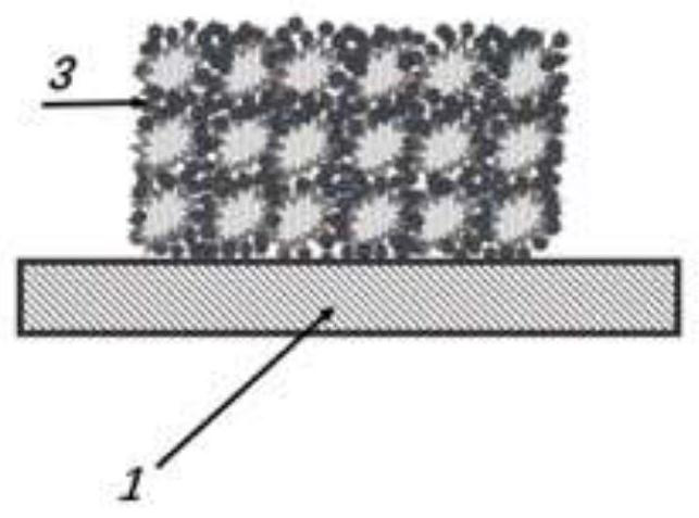
[0046] refer to figure 1 and figure 2 , the present invention provides a kind of compound structure lead salt thin film, 1 is substrate, 2 is the lead salt grain layer of loose structure prepared by physical vapor deposition method, 3 is the small grain lead salt of chemical method growth;

[0047] Wherein, the lead salt grain layer is covered on the substrate, and there are gaps between the lead salt grains;

[0048] Wherein, the small grain lead salt is embedded in the gap between the lead salt grains of the lead salt grain layer;

[0049] Wherein, the lead salt is lead sulfide or lead selenide;

[0050] Wherein, the substrate is a quartz substrate or a sapphire substrate or a silicon wafer containing an oxide layer.

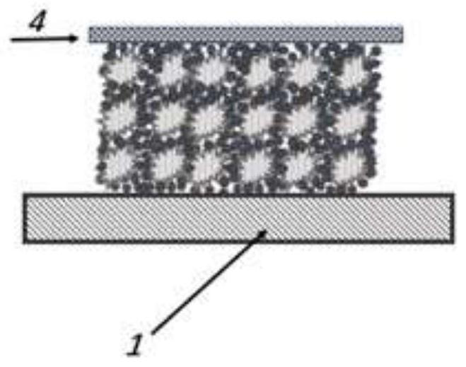
[0051] refer to image 3 , 4 is the passivation layer, after annealing the lead salt thin film of the composite structure, a passivation layer is added, and the passivation layer is bonde...

Embodiment 2

[0052] The preparation of embodiment 2 composite structure lead selenide film

[0053] (1) physical vapor deposition

[0054] The quartz substrate is cut into a regular size (such as 4*2.5cm2), cleaned, and multiple pieces of quartz are placed in a fixture and placed in a vapor deposition furnace;

[0055] Add polycrystalline lead selenide into the crucible, close the furnace hall, and evacuate to 10-4Pa level;

[0056] Heating the crucible to melt the lead selenide to volatilize it;

[0057] According to the thickness parameters of the film thickness meter, the thickness of the lead selenide film is 0.9-1.1um;

[0058] Turn off the heating power supply, fill with nitrogen gas to normal pressure, open the furnace, and take out the quartz plate with lead selenide film.

[0059] (2) Chemical water bath

[0060] Adopt 99.99% pure selenium powder (5g) and 99% pure sodium sulfite (7.98g) and high-purity water 600mL to configure sodium selenosulfate solution, stir for 24 hours, ...

Embodiment 3

[0072] Embodiment 3 product test

[0073] The chip formed through the step-by-step processing of the embodiment 2 can be used for spot welding packaging to form a lead selenide detector with excellent performance.

[0074] Noise test and photoelectric response test were carried out on the lead selenide detector. The noise test results are as follows: Figure 4 As shown; and using a 500K black body light source, the photoelectric response test results are as follows Figure 5 shown.

[0075] The result shows that the noise of the device is extremely low. Compared with existing market products, the noise of the lead-salt detector of the present invention is 1-2 orders of magnitude lower, and the specific detection rate reaches 5.5*10 10 Jones, compared with similar foreign products Laser Components lead selenide detector (1.8*10 10 Jones) is about 200% higher than that of Sorebo's similar lead selenide products (2.5*10 9 Jones) more than 10 times higher. In particular, the ...


PUM


Abstract

The invention belongs to the field of photoelectronic devices, and particularly relates to a composite-structure lead salt film for infrared photoelectricity and a preparation method thereof. The leadsalt film comprises a base, a lead salt crystal grain layer prepared by a physical vapor deposition method, and small-crystal-grain lead salt prepared by a chemical method; the lead salt crystal grain layer covers the base, and gaps exist among lead salt crystal grains; the small-crystal-grain lead salt is embedded into the gaps; the lead salt film is lead sulfide or lead selenide; and the base is a quartz substrate or a sapphire substrate or a silicon wafer containing an oxide layer. The preparation method comprises a physical vapor deposition method and a chemical method. The composite structure lead salt film provided by the invention is more compact in structure and high in uniformity; as a photoelectric detector, the annealed composite structure lead salt film is low in noise, high in specific detection rate, short in time consumption of the preparation method and simple in process.

Description

technical field [0001] The invention belongs to the field of optoelectronic devices, and in particular relates to a composite structure lead salt thin film and a preparation method thereof. Background technique [0002] A photodetector is an electronic device that converts optical signals into electrical signals. It is used in the ultraviolet and infrared bands invisible to the human eye, and in occasions and scenes that cannot be reached by human beings, such as dark fields at night, high-temperature and high-risk environments, and uninterrupted surveillance. have important applications. Infrared detectors realize photoelectric detection in the infrared band. Currently, there are two principles: photon type and photothermal type. The photonic infrared detector has a fast response speed, and the photothermal infrared detector has a wide response band, each with its own advantages. [0003] Lead salt (PbS / PbSe), as a narrow bandgap semiconductor material with NaCl structure...

Claims


Application Information

Patent Timeline
Patent Type & Authority Applications(China)
IPC IPC(8): H01L31/09H01L31/032H01L21/02H01L31/18
CPCH01L21/02568H01L21/02628H01L21/02631H01L31/0324H01L31/09H01L31/1864Y02P70/50
Inventor 周大华李云杰黄德萍冯双龙杨俊孙泰史浩飞
Owner CHONGQING INST OF GREEN & INTELLIGENT TECH CHINESE ACADEMY OF SCI
Why Eureka
Try Eureka