Preparation method of low-thermal-resistance gallium nitride high-electron-mobility transistor epitaxial material

A technology of high electron mobility and epitaxial materials, which is applied in the field of epitaxial material preparation of GaN high electron mobility transistors with low thermal resistance, can solve the performance deterioration of device output power density and efficiency, lattice mismatch, increase aluminum nitride Thermal resistance and other issues, to achieve stable and controllable high-temperature etching technology, avoid material performance differences, and reduce the effect of interface thermal resistance

Active Publication Date: 2021-04-16
NO 55 INST CHINA ELECTRONIC SCI & TECHNOLOGYGROUP CO LTD
View PDF5 Cites 6 Cited by
  • Summary
  • Abstract
  • Description
  • Claims
  • Application Information

AI Technical Summary

Problems solved by technology

[0003] Because there is a certain lattice mismatch between aluminum nitride and silicon carbide, and the aluminum-nitrogen bond energy is large, the aluminum nitride grows in an island shape, and a large number of defects are introduced in the process of merging between the islands, resulting in nitrogen The aluminum nitride lattice is poor, so that the thermal conductivity of the aluminum nitride nucleation layer is much lower than the theoretical value, even lower than other functional layers
In addition, in order to ensure the crystal quality of gallium nitride and the impurity shielding effect of aluminum nitride, the thickness of the nucleation layer of aluminum nitride is generally not less than 50nm, which further increases the thermal resistance of aluminum nitride and forms an obvious boundary thermal resistance, which seriously Limits heat transfer from the channel to the substrate side
While the power of GaN microwave power devices is increasing, the device junction temperature rises significantly, resulting in rapid deterioration of device output power density and efficiency. The problem of heat dissipation has become the biggest limitation to the further development and application of SiC-based GaN microwave power device technology. bottleneck

Method used


Image

  • Preparation method of low-thermal-resistance gallium nitride high-electron-mobility transistor epitaxial material
  • Preparation method of low-thermal-resistance gallium nitride high-electron-mobility transistor epitaxial material
  • Preparation method of low-thermal-resistance gallium nitride high-electron-mobility transistor epitaxial material

Examples


specific Embodiment approach

[0030] Step 1: Select a silicon carbide single crystal substrate and place it on the base in the reaction chamber of the high temperature chemical vapor deposition equipment;

[0031] Step 2: Set the pressure of the reaction chamber to 100~200 mbar, and inject H 2 , the temperature of the reaction chamber is raised to 1000~1100°C, under H 2 Bake the substrate under atmosphere for 5-15 minutes to remove surface contamination;

[0032] Step 3: Maintain H 2 The flow rate and the pressure of the reaction chamber remain unchanged, and the temperature of the reaction chamber is raised to 1300~1600°C. 2 Etch the substrate for 5-15 minutes under the atmosphere, so that the surface of the substrate presents an atomic step morphology;

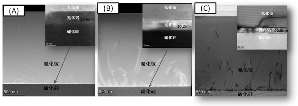
[0033] Step 4: Maintain H 2 The flow rate is constant, the pressure of the reaction chamber is set at 50~150 mbar, the temperature of the reaction chamber is set at 1100~1150°C, and NH 3 and an aluminum source to grow an aluminum nitride atomic depo...

Embodiment

[0046] Provided in a CVD (Chemical Vapor Deposition) system and an MOCVD (Metal Organic Compound Vapor Deposition) system is an epitaxial method for reducing the interface thermal resistance of GaN high electron mobility transistors, including the following steps:

[0047] Step 1: Select a 4-inch silicon carbide single crystal substrate and place it on the base in the CVD equipment.

[0048] Step 2: Set the reaction chamber pressure to 100mbar, H 2 With a flow rate of 100 slm, the temperature of the system was raised to 1080°C and held for 5 minutes to perform high-temperature cleaning on the substrate surface.

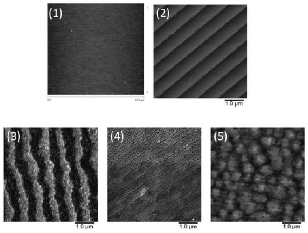
[0049] Step 3: Maintain the reaction chamber pressure and H 2 The flow rate remains unchanged, and the temperature continues to rise to 1500°C. 2 The substrate was etched for 10 minutes under the atmosphere, so that the surface of the substrate showed atomic step morphology.

[0050] Step 4: After the etching is completed, in the H 2 The temperature is lowered in ...


PUM

PropertyMeasurementUnit
thicknessaaaaaaaaaa
thicknessaaaaaaaaaa
thicknessaaaaaaaaaa

Abstract

The invention discloses a preparation method of a low-thermal-resistance gallium nitride high-electron-mobility transistor epitaxial material, and belongs to the technical field of semiconductor epitaxial materials. According to the invention, the method comprises the steps: employing high-temperature chemical vapor deposition equipment for carrying out high-temperature etching on the surface of a silicon carbide substrate, so the surface of the substrate presents controllable atomic-scale step morphology; carrying out the atomic-scale aluminum nitride nucleation on silicon carbide atomic steps by utilizing a metal organic chemical vapor deposition technology; transversely and rapidly combining the aluminum nitride nucleation points in an intermittent source supply mode, and performing layered deposition, so high-quality nanoscale aluminum nitride nucleation layer growth is achieved, and the gallium nitride high-electron-mobility transistor is prepared by taking aluminum nitride as a substrate. According to the method, the thickness of the aluminum nitride nucleating layer can be greatly reduced, the interface thermal resistance introduced by the aluminum nitride nucleating layer can be effectively reduced, the heat dissipation characteristic of the gallium nitride power device can be improved, and the method has extremely important significance for improving the power performance of the gallium nitride microwave power device.

Description

technical field [0001] The invention relates to a method for preparing epitaxial materials for transistors with low thermal resistance gallium nitride and high electron mobility, and belongs to the technical field of semiconductor epitaxial materials. Background technique [0002] Gallium nitride material has properties such as wide direct band gap, strong atomic bond, high thermal conductivity, good chemical stability (hardly corroded by any acid) and strong radiation resistance, which can meet the needs of next-generation power devices Application requirements such as higher power density, higher operating frequency, smaller size and harsher environment are the important foundation and key support for the manufacture of GaN microwave power devices and circuits. Since silicon carbide substrates have higher thermal conductivity and smaller lattice mismatch, current high-power gallium nitride power transistors usually use silicon carbide-based gallium nitride high electron mo...

Claims


Application Information

Patent Timeline
Patent Type & Authority Applications(China)
IPC IPC(8): H01L21/02H01L29/778
Inventor 张东国李忠辉
Owner NO 55 INST CHINA ELECTRONIC SCI & TECHNOLOGYGROUP CO LTD
Why Eureka
Try Eureka