

Preparation method of SERS substrate based on 2D noble metal nanostructure
A nanostructure, precious metal technology, applied in metal material coating process, ion implantation plating, coating and other directions, can solve the problems of difficult to prepare plasmonic nanostructure array, difficult to evenly distribute hot spots, etc., to improve detection Sensitivity, excellent repeatability and stability, good periodicity
- Summary
- Abstract
- Description
- Claims
- Application Information
AI Technical Summary
Problems solved by technology
Method used
Image

Examples
Embodiment 1
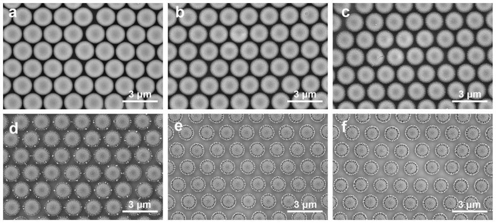
[0034] This embodiment provides a method for processing a SERS substrate based on a 2D noble metal nanostructure, which specifically includes the following steps:
[0035] S1, the surface is deposited with 300nm silicon oxide single crystal silicon (referred to as SiO 2 / Si) The substrate is successively placed in acetone, absolute ethanol and deionized water for ultrasonic cleaning for 10 minutes, taken out and dried with nitrogen, and treated with an ultraviolet ozone system for 30 minutes to make the surface of the substrate exhibit superhydrophilic properties;
[0036]S2. Using the colloidal self-assembly method to self-assemble a layer of polystyrene (PS) microsphere arrays in a regular and orderly arrangement on the surface of the substrate after step S1, and then place the substrate in a drying oven at 60°C for drying treatment 90min, and then further increase the temperature to 80°C for 5min heat treatment to obtain substrate A;
[0037] In the step S2, the specific s...
Embodiment 2
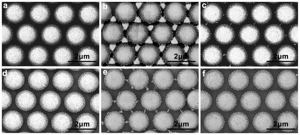
[0046] This embodiment provides a method for processing a SERS substrate based on a 2D noble metal nanostructure, which specifically includes the following steps:
[0047] S1, put 2 pieces of SiO 2 The / Si substrate was placed in acetone, absolute ethanol, and deionized water for 8 minutes to be ultrasonically cleaned, taken out and dried with nitrogen, and then treated with an ultraviolet ozone system for 25 minutes to make the surface of the substrate appear super-hydrophilic;
[0048] S2. Using the colloidal self-assembly method to self-assemble a layer of polystyrene (PS) microsphere arrays in a regular and orderly arrangement on the surface of the substrate after step S1, and then place the substrate in a drying oven at 60°C for drying treatment After 60 minutes, the temperature was further raised to 80°C for 5 minutes of heat treatment to obtain substrate A;
[0049] S3, using a plasma etching machine to carry out oxygen plasma etching on the substrate A prepared in ste...
PUM
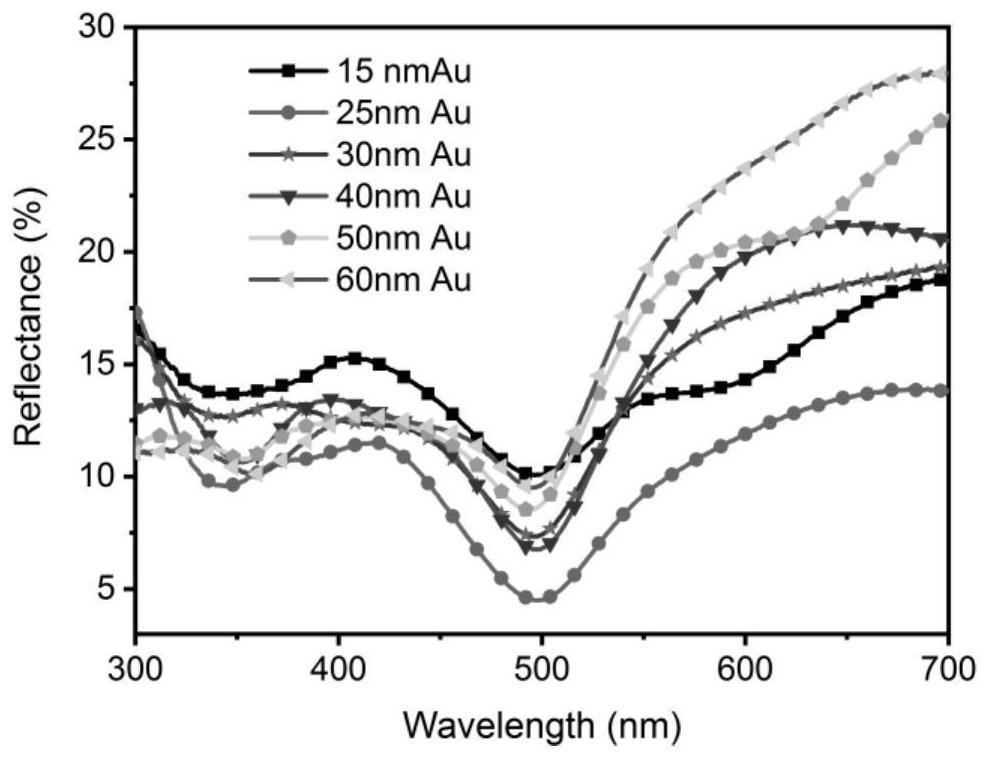
| Property | Measurement | Unit |
|---|---|---|
| diameter | aaaaa | aaaaa |
| porosity | aaaaa | aaaaa |
| reflectance | aaaaa | aaaaa |
Abstract
Description
Claims
Application Information