MWT heterojunction solar cell and preparation method thereof

A heterojunction battery and battery technology, applied in circuits, photovoltaic power generation, electrical components, etc., can solve the problems of reduced PN junction effective area, large PN junction failure area, and reduced battery efficiency, so as to improve the passivation effect and improve Effect of opening pressure, conversion efficiency, and area reduction

Pending Publication Date: 2021-07-13
JIANGSU SUNPORT POWER CORP LTD
View PDF1 Cites 11 Cited by
  • Summary
  • Abstract
  • Description
  • Claims
  • Application Information

AI Technical Summary

Problems solved by technology

However, laser isolation inevitably has thermal damage, which has an adverse effect on battery passivation, resulting in a decrease in battery efficiency, and to achieve insulation isolation requires a wider scribe width, resulting in a larger failure area of ​​​​the PN junction and a decrease in the effective area of ​​​​the PN junction.

Method used


Image

  • MWT heterojunction solar cell and preparation method thereof

Examples


Embodiment 1

[0028] Embodiment 1: experimental group

[0029] 1. Silicon wafer: use N-type single crystal silicon wafer as the substrate

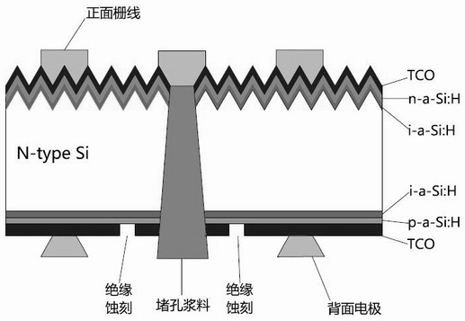
[0030] 2. Laser drilling: According to the 6×6 hole dot matrix pattern, holes are drilled on the silicon wafer to form circular holes with a diameter of 0.2mm.

[0031] 3. Polishing and oxidation: Polish the silicon wafer on both sides after drilling, use tubular thermal oxygen oxidation on the front of the silicon wafer, the oxidation temperature is 180°C, the oxygen flow rate is 2000 sccm, and a 5nm oxide layer is formed on the front

[0032] 4. Texturing and cleaning: Alkali and single-sided texturing additive (TS03) are used for single-sided texturing to remove the damaged layer on the surface of the silicon wafer and reduce the recombination rate of photogenerated carriers; at the same time, uniform texture is formed on the front side of the silicon wafer The surface can trap light and improve light absorption; RCA cleaning improves the cleanlines...

Embodiment 2

[0039] Embodiment 2: comparison group

[0040] 1. Silicon wafer: use N-type single crystal silicon wafer as the substrate

[0041] 2. Laser drilling: According to the 6×6 hole dot matrix pattern, holes are drilled on the silicon wafer to form circular holes with a diameter of 0.2mm.

[0042] 3. Texture making and cleaning: Alkali and conventional texturing additives (TS01) are used for double-sided texturing to remove the damaged layer on the surface of the silicon wafer and reduce the recombination rate of photogenerated carriers; at the same time, a uniform textured surface is formed on the front side of the silicon wafer , can play the role of trapping light and improve the absorption of light; RCA cleaning improves the cleanliness of the silicon wafer surface.

[0043] 4. Intrinsic amorphous silicon layer deposition: use PECVD to deposit 3nm intrinsic amorphous silicon film on the front and back of the silicon wafer

[0044] 5. Deposition of N-type amorphous silicon on t...


PUM

PropertyMeasurementUnit
diameteraaaaaaaaaa
diameteraaaaaaaaaa

Abstract

The invention discloses an MWT heterojunction solar cell and a preparation method thereof, the MWT heterojunction solar cell sequentially comprises a front conductive TCO layer, a front N-type doped amorphous silicon layer, a front intrinsic amorphous silicon layer, a monocrystalline silicon substrate, a back intrinsic amorphous silicon layer, a back P-type doped amorphous silicon layer and a back TCO conductive layer, the front surface is a textured structure, and the back surface is a polished surface. According to the preparation method of the cell provided by the invention, the special etching slurry for the TCO is used for insulating the conductive TCO between the positive electrode and the negative electrode of the back surface to replace laser insulation, so that the insulation effect is better, the electric leakage failure ratio is reduced, the yield is improved, the damage of laser insulation isolation to a silicon substrate can be avoided, and the open voltage and conversion efficiency of the MWT heterojunction cell are improved.

Description

technical field [0001] The invention relates to a MWT heterojunction solar cell suitable for mass production and a preparation method thereof, belonging to the field of silicon-based solar cell manufacturing. Background technique [0002] MWT is a metal perforation and winding technology, which is applied in solar cells. It uses laser or other methods to realize the perforation process on the original silicon wafer, so as to achieve the purpose of leading the positive and negative electrodes to the same surface. The unique busbar-free design reduces the increase in the shading area. The current density of the battery can improve the conversion efficiency; the heterojunction silicon-based battery is a kind of high-efficiency photovoltaic battery, generally using N-type silicon wafer with high minority carrier life, combined with intrinsic amorphous silicon passivation layer and P-type amorphous silicon doped The heterogeneous PN junction structure is obtained for the heteroge...

Claims


Application Information

Patent Timeline
Patent Type & Authority Applications(China)
IPC IPC(8): H01L31/0352H01L31/0224H01L31/0747H01L31/20
CPCH01L31/02245H01L31/035281H01L31/0747H01L31/202Y02E10/50Y02P70/50
Inventor 刘晓瑞王伟逯好峰吴仕梁路忠林张凤鸣
Owner JIANGSU SUNPORT POWER CORP LTD
Why Eureka
Try Eureka