Preparation method of phosphorus-selenium co-doped niobium disulfide nano material
A technology of niobium disulfide and nanomaterials, applied in chemical instruments and methods, inorganic chemistry, niobium compounds, etc., to achieve the effects of overcoming uneven product morphology, high purity and simple production process
- Summary
- Abstract
- Description
- Claims
- Application Information
AI Technical Summary
Problems solved by technology
Method used
Image
Examples
Embodiment 1
[0035] Example 1 Preparation of phosphorus-selenium co-doped niobium disulfide nanoflowers
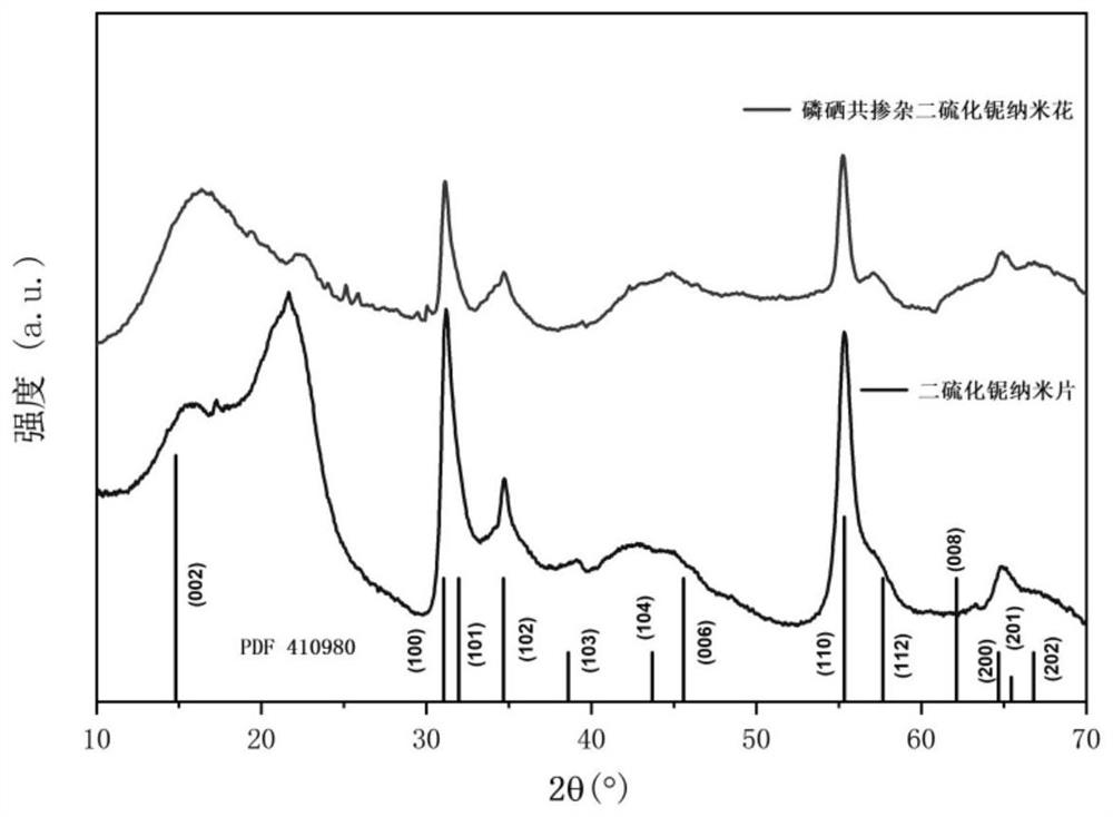
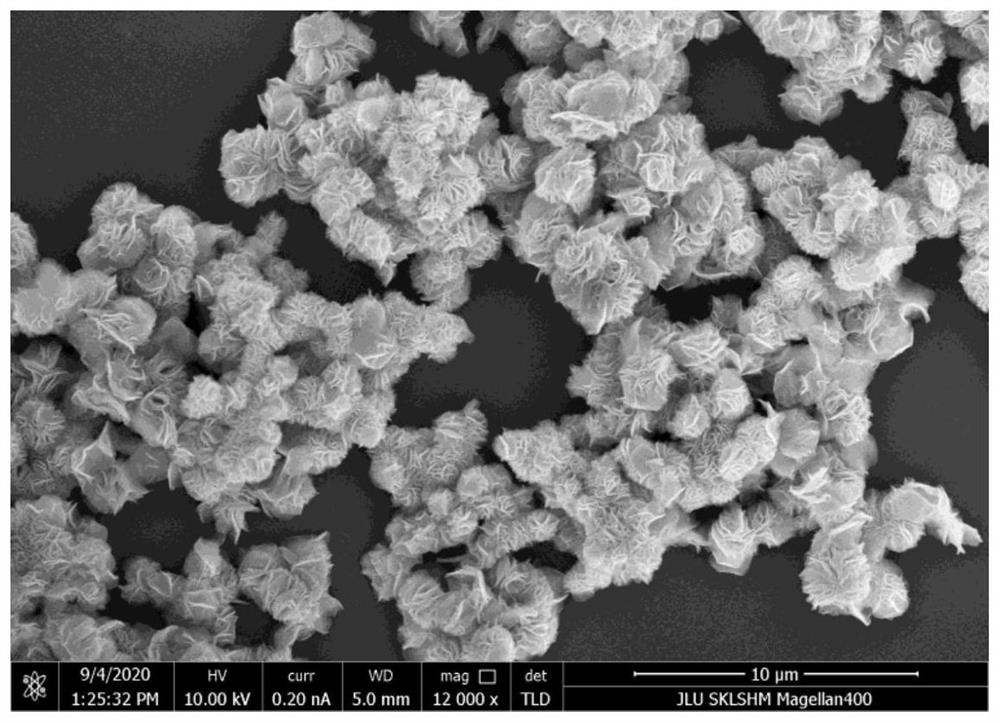
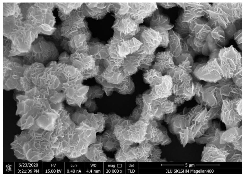
[0036] Put 4mL of oleylamine into a three-necked flask for magnetic stirring, raise the temperature to 130°C under the protection of nitrogen, keep it for 20 minutes, then cool down naturally, put 1.6mmol of niobium pentachloride and degassed oleylamine in the three-necked flask Mix in medium and magnetically stir, raise the temperature to 300°C under the protection of nitrogen, inject 8mmol CS 2 Sulfur source, kept at this temperature for 2 hours, then naturally lowered to 200°C, injected the prepared TOP-Se (1mmol-0.3mmol) solution, the system temperature rose rapidly to 320°C, kept for 1 hour, and the reaction ended , the solution was naturally cooled to room temperature, washed with n-hexane and methanol, and then freeze-dried. like figure 1 As shown, the X-ray diffraction spectrum picture (XRD) of phosphorus-selenide co-doped niobium disulfide nanoflowers is very well compared w...
Embodiment 2 2
[0037] The preparation of embodiment 2 niobium disulfide nanosheets
[0038] Put 4 mL of oleylamine and 1.6 mmol of niobium pentachloride into a three-neck flask for magnetic stirring, and raise the temperature to 300 °C at a rate of 5 °C / min under the protection of nitrogen, and inject 8 mmol of CS 2 The sulfur source was kept at this temperature for 3 hours, then the temperature was naturally lowered, the solution was naturally cooled to room temperature, the sample was washed with n-hexane and methanol, and then freeze-dried. Figure 6~7 Scanning electron micrographs with scale bars of 3 μm and 2 μm, respectively, which are obviously different from nanoflowers and evenly distributed. Figure 8-9 Transmission electron micrographs with scale bars of 500 nm and 200 nm, respectively. It is clearly seen that NbS 2 Nanosheets and NbS 2 Nanoflowers have a smaller diameter in comparison, about 200nm.
[0039] The phosphorus-selenium co-doped niobium disulfide nanoflowers and ni...
Embodiment 3
[0040] Embodiment 3 electrocatalytic hydrogen evolution performance test
[0041] Electrochemical catalytic properties of phosphorus-selenide co-doped niobium disulfide nanoflowers and niobium disulfide nanosheets were measured by electrochemical workstation. like Figure 20As shown, it is phosphorus selenium co-doped niobium disulfide nanoflowers, niobium disulfide nanosheets in acidic solution 0.5MH 2 SO 4 Linear sweep voltammetry curves and Tafel slope curves in . It can be seen that after the regulation of morphology and the influence of phosphorus-selenium co-doping, at 10mA cm -2 The overpotential increased from -0.534V of NBS nanosheets to -0.368V of P-Se co-doped NbS nanoflowers under the current density of -0.585V. The current density of nanoflowers can reach 130mA cm -2 , while at the same overpotential, the current density of niobium disulfide nanosheets is only 13.8mAcm -2 . like Figure 21 As shown, the change of Tafel slope is also obvious, from 406.4mV / d...
PUM
| Property | Measurement | Unit |
|---|---|---|
| diameter | aaaaa | aaaaa |
Abstract
Description
Claims
Application Information
 - R&D
- Intellectual Property
- Life Sciences
- Materials
- Tech Scout
- Unparalleled Data Quality
- Higher Quality Content
- 60% Fewer Hallucinations
Browse by: Latest US Patents, China's latest patents, Technical Efficacy Thesaurus, Application Domain, Technology Topic, Popular Technical Reports.
© 2025 PatSnap. All rights reserved.Legal|Privacy policy|Modern Slavery Act Transparency Statement|Sitemap|About US| Contact US: help@patsnap.com


