Semiconductor material, field effect transistor device, bipolar semiconductor and application
A field-effect transistor and semiconductor technology, applied in semiconductor devices, semiconductor/solid-state device manufacturing, electric solid-state devices, etc., to achieve the effect of reducing energy gap, promoting orbital distribution, and promoting effective transmission
- Summary
- Abstract
- Description
- Claims
- Application Information
AI Technical Summary
Problems solved by technology
Method used
Image
Examples
preparation example Construction
[0037] The invention provides a method for preparing a semiconductor material, comprising:
[0038] Synthesis of D-A-D-type flying fish-like molecules; through the electronic effect of side groups, the energy gap is reduced and the energy level distribution of HUMO-LUMO is adjusted to match the Fermi level of the metal electrode to promote the effective injection of charges;
[0039] Preparation of crystal materials formed by crossed dipole molecular packing with strong π-π interaction in close distance.
[0040] The synthesis of D-A-D flying fish-like molecules includes:
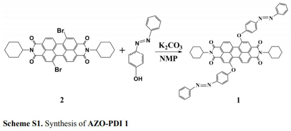
[0041] The perylene diimide core PDI is used as the electron acceptor, and the two azophenoxy groups in the bay position are used as electron donors to form a D-A-D type flying fish-like molecular structure; through chemical modification, the weak electron donor of the two azophenol groups is used Effect, so that the HOMO-LUMO energy level difference of the whole molecule is reduced, and its HOMO and LUMO ...
Embodiment 1
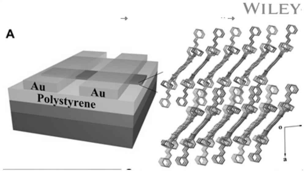
[0049] Such as figure 1 , a one-dimensional nanoribbon single crystal as the semiconductor charge transport layer to prepare the corresponding bottom gate, top contact mode field effect transistor device, with n-type silicon as the substrate and gate, 400nm thick SiO 2 For the insulating layer, the polystyrene film was modified by the spin-coating method, and the methanol suspension containing an appropriate amount of single-crystal micro-belts was dropped onto the surface, dried in vacuum overnight, and metal gold was thermally evaporated onto the nano-belts by the mask method. The two ends are used as the source and the drain, and the corresponding field effect transistor device is made, and its field effect performance is tested, and its hole mobility is measured to be 6.74cm 2 V -1 the s -1 ; The electron mobility is 5.96cm 2 V -1 the s -1 ; single crystal microstrips exhibit an average electron and hole mobility of about 0.1 cm in ambient atmosphere 2 v -1 the s ...
Embodiment 2
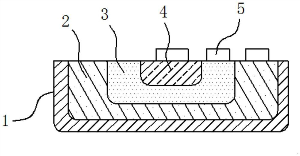
[0051] A bipolar semiconductor device, comprising a substrate bushing 1, an anode 2 is fixed on the upper layer of the substrate bushing 1, an emission layer 3 is fixed on the upper part of the anode 2, a cathode 4 is fixed on the upper part of the emission layer 3, and the emission layer 3 is the use of an organic semiconductor compound AzoO 2 -Crystal material formed by PDIs, the general chemical structure formula of the compound is: C 60 h 46 N 6 o 6 ;
[0052] The organic semiconductor compound is formed by compounding one molecule of perylenetetracarboxylic anhydride, two molecules of cyclohexane and two molecules of azophenol;
[0053] Two molecules of cyclohexane dehydrate and condense with the acid anhydrides on both sides of perylene tetracarboxylic anhydride to form corresponding perylene diimides, and two molecules of azophenol react with 1,7-dibromoperylene imides respectively. bit condensed;
[0054] When in use, the junction block 5 is electrically connecte...
PUM
| Property | Measurement | Unit |
|---|---|---|
| Hole mobility | aaaaa | aaaaa |
| Electron mobility | aaaaa | aaaaa |
| Hole mobility | aaaaa | aaaaa |
Abstract
Description
Claims
Application Information


