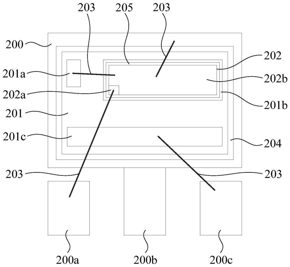
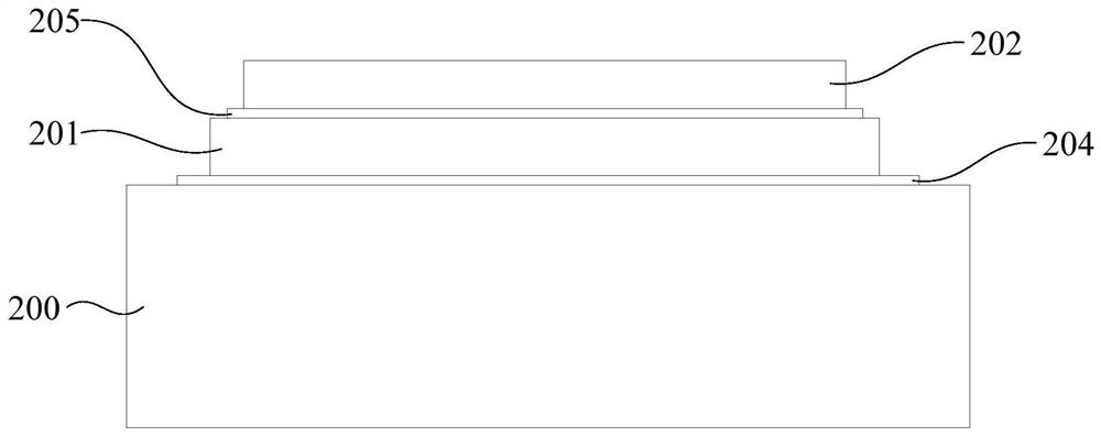
Gallium nitride device packaging structure
A device packaging and gallium nitride technology, which is applied in semiconductor devices, electrical solid state devices, semiconductor/solid state device components, etc., can solve problems such as the inability to effectively reduce the packaging area, increase the parasitic inductance of the device, and reduce the switching performance of the device
- Summary
- Abstract
- Description
- Claims
- Application Information
AI Technical Summary
Problems solved by technology
Method used
Image
Examples
Embodiment 1
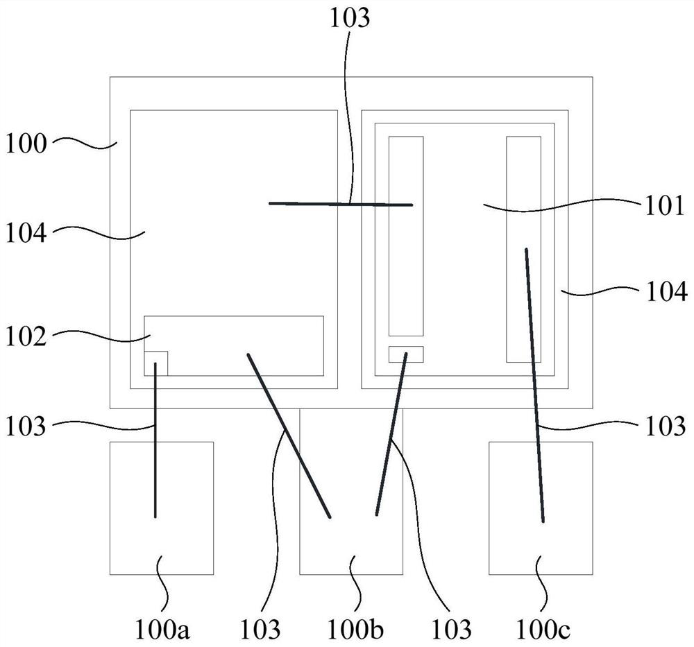
[0082] Such as figure 1 As shown in FIG. 2 , it is a schematic top view of the GaN device packaging structure in the prior art. exist figure 1 Among them, a gallium nitride high electron mobility transistor chip 101 and a silicon metal oxide semiconductor field effect transistor chip 102 are packaged on the lead frame 100 respectively, and are connected by wires 103 . The gallium nitride high electron mobility transistor chip 101 and the silicon metal oxide semiconductor field effect transistor chip 102 are also respectively connected to the gate pin 100a, the source pin 100b and the drain of the lead frame 100 Pin 100c. In the above packaging structure, the two kinds of chips are respectively placed on the DBC board 104 . The existence of the DBC board 104 not only increases the thermal conduction path of the device, thereby increasing the thermal resistance of the device, but also increases the packaging cost. Due to the limited substrate area of the lead frame 100, th...
Embodiment 2
[0092] The package form adopted by the gallium nitride device package structure provided by the present invention is not limited to the in-line TO package, but also includes SMD TO package, QFN package, DFN package, TOLL package, SOP package or SOIC package and other package forms. .
[0093] For example, if Figure 4 As shown, this embodiment also provides a GaN device packaging structure. Compared with the TO packaging structure provided in Embodiment 1, the difference of this embodiment is that the TOLL packaging form is adopted.
[0094] Specifically, such as Figure 4 As shown, in the GaN device packaging structure adopting the TOLL packaging structure, the first chip 301 and the second chip 302 are sequentially stacked on the lead frame 300 . Wherein, the first chip 301 includes a high voltage depletion gallium nitride high electron mobility transistor (GaN HEMT), and the second chip 302 includes a low voltage enhancement type silicon metal oxide semiconductor field ef...
Embodiment 3
[0100] Such as Figure 5 As shown, this embodiment provides a gallium nitride device packaging structure. Compared with the first embodiment, the difference of this embodiment is that a QFN packaging form is adopted.
[0101] Specifically, such as Figure 5As shown, in the GaN device package structure using the QFN package structure, the first chip 401 and the second chip 402 are sequentially stacked on the lead frame 400 . Wherein, the first chip 401 includes a high voltage depletion gallium nitride high electron mobility transistor (GaN HEMT), and the second chip 402 includes a low voltage enhancement type silicon metal oxide semiconductor field effect transistor (Si MOSFET). The gate 401a, source 401b and drain 401c of the gallium nitride high electron mobility transistor are located on the front side of the first chip 401; the gate 402a and source of the silicon-based metal oxide semiconductor field effect transistor 402b is located on the front side of the second chip 4...
PUM
 Abstract
Description
Claims
Application Information
 - R&D Engineer
- R&D Manager
- IP Professional
- Industry Leading Data Capabilities
- Powerful AI technology
- Patent DNA Extraction
Browse by: Latest US Patents, China's latest patents, Technical Efficacy Thesaurus, Application Domain, Technology Topic, Popular Technical Reports.
© 2024 PatSnap. All rights reserved.Legal|Privacy policy|Modern Slavery Act Transparency Statement|Sitemap|About US| Contact US: help@patsnap.com


