
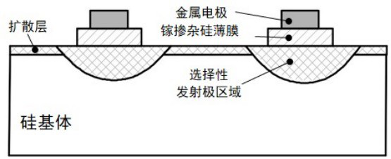
Method for preparing selective emitter by using gallium-doped silicon nano slurry

A nano-slurry, doped silicon technology, applied in photovoltaic power generation, climate sustainability, final product manufacturing, etc., can solve the problems of high cost, high temperature thermal damage of boron diffusion in production equipment, and improvement of solar cell performance, etc. High, improve the minority carrier lifetime, improve the effect of battery performance

Pending Publication Date: 2021-10-01
YANCHENG INST OF TECH
View PDF5 Cites 0 Cited by
  • Summary
  • Abstract
  • Description
  • Claims
  • Application Information

AI Technical Summary

Problems solved by technology

[0004] The invention discloses a low-cost, compatible with the current technology, industrialized production and high productivity method for preparing selective emitters using gallium-doped silicon nano-slurry, which overcomes the high cost and special production requirements in the prior art Equipment and high temperature thermal damage caused by boron diffusion, and then solve the problem that restricts the performance improvement of solar cells

Method used


Image

  • Method for preparing selective emitter by using gallium-doped silicon nano slurry
  • Method for preparing selective emitter by using gallium-doped silicon nano slurry
  • Method for preparing selective emitter by using gallium-doped silicon nano slurry

Examples


Embodiment 1

[0032] This embodiment provides a method for preparing a selective emitter by using gallium-doped silicon nano-slurry. The gallium-doped silicon nano-slurry used is prepared by mixing gallium-doped nano-silicon particles and an organic carrier. The gallium-doped silicon nano-slurry is used as raw material, the pattern is printed by a screen printing machine, and the selective emitter is prepared by laser-assisted diffusion. Specific steps are as follows:

[0033] Step 1: Select a phosphorus-doped N-type single crystal silicon wafer with a resistivity of 0.5-2Ω·cm, place it in a texturing tank, and place it in a sodium hydroxide solution with a specific gravity of 5-15%. Under the condition of 75 ~ 80 ℃, the surface texture is formed to form a suede structure;

[0034] Step 2: Clean the surface of the silicon wafer with a chemical solution, the solution is a mixed solution of hydrofluoric acid and hydrochloric acid, the cleaning time is 2Min, and the temperature is 20-25°C;

...

Embodiment 2

[0048] This embodiment provides a method for preparing a selective emitter by using gallium-doped silicon nano-slurry. The gallium-doped silicon nano-slurry used is prepared by mixing gallium-doped nano-silicon particles and an organic carrier. The gallium-doped silicon nano-slurry is used as raw material, the pattern is printed by a screen printing machine, and the selective emitter is prepared by laser-assisted diffusion. Specific steps are as follows:

[0049] Step 1: Select a phosphorus-doped N-type single crystal silicon wafer with a resistivity of 0.5-2Ω·cm, place it in a texturing tank, and place it in a sodium hydroxide solution with a specific gravity of 5-15%. Under the condition of 75 ~ 80 ℃, the surface texture is formed to form a suede structure;

[0050] Step 2: Clean the surface of the silicon wafer with a chemical solution, the solution is a mixed solution of hydrofluoric acid and hydrochloric acid, the cleaning time is 2Min, and the temperature is 20-25°C;

...

Embodiment 3

[0064] This embodiment provides a method for preparing a selective emitter by using gallium-doped silicon nano-slurry. The gallium-doped silicon nano-slurry used is prepared by mixing gallium-doped nano-silicon particles and an organic carrier. The gallium-doped silicon nano-slurry is used as raw material, the pattern is printed by a screen printing machine, and the selective emitter is prepared by laser-assisted diffusion. Specific steps are as follows:

[0065] Step 1: Select a phosphorus-doped N-type single crystal silicon wafer with a resistivity of 0.5-2Ω·cm, place it in a texturing tank, and place it in a sodium hydroxide solution with a specific gravity of 5-15%. Under the condition of 75 ~ 80 ℃, the surface texture is formed to form a suede structure;

[0066] Step 2: Clean the surface of the silicon wafer with a chemical solution, the solution is a mixed solution of hydrofluoric acid and hydrochloric acid, the cleaning time is 2Min, and the temperature is 20-25°C;

...


PUM

PropertyMeasurementUnit
Sizeaaaaaaaaaa
Thicknessaaaaaaaaaa
Sizeaaaaaaaaaa

Abstract

The invention discloses a method for preparing a selective emitter by using a gallium-doped silicon nano slurry. The method comprises the following steps of transferring patterns on the front surface of a diffused crystalline silicon solar cell by using a slurry prepared from gallium-doped silicon nano particles as a doping source and adopting silk-screen printing, and drying to form a gallium-doped silicon nano film; and forming a selective diffusion area with local heavily doped gallium on the front surface of the cell by adopting a laser-assisted diffusion process, and then finally obtaining the solar cell with a selective emitter through subsequent solar cell processes such as cleaning of redundant doping sources and overprinting of metal electrodes. The preparation method of the selective emitter can be completely compatible with an existing solar cell production process, new equipment does not need to be added, the production cost is low, and the preparation method is suitable for industrial production.

Description

technical field [0001] The invention relates to the technical field of solar cell preparation, in particular to a method for preparing a selective emitter using gallium-doped silicon nano-slurry. Background technique [0002] Among the hot issues in today's solar energy research, tunneling oxide passivation contact (TOPCon) technology has become one of the key research directions for industrialized high-efficiency solar cells. It is reported that the highest conversion efficiency of N-type TOPCon cells has reached 25.8%. For N-type batteries, the p+ emitter region is formed after shallow diffusion on the front surface, and the metal contact is formed after the metal electrode is screen-printed, dried and sintered. Due to the direct contact between the metal electrode and the silicon substrate, compound damage to the metal contact is formed, resulting in The carrier recombination is serious, which is reflected in the dark saturation current density in the contact area (J 0,...

Claims


Application Information

Patent Timeline
IPC IPC(8): H01L31/0392H01L31/0224H01L31/18
CPCH01L31/0392H01L31/022425H01L31/18Y02P70/50Y02E10/50
Inventor 洪捐张泽新王玉杰夏梁冬许伟良
Owner YANCHENG INST OF TECH
Learn More