Graphene/gallium arsenide solar cell with array micro-nano lens structure and preparation method of graphene/gallium arsenide solar cell

A lens structure and solar cell technology, which is applied in the field of solar cells, can solve the problems of complex manufacturing process, low efficiency, and high cost, and achieve the effects of convenient preparation, wide application range, and anti-oxidation

Pending Publication Date: 2021-11-23
SOUTH CHINA UNIV OF TECH
View PDF0 Cites 0 Cited by
  • Summary
  • Abstract
  • Description
  • Claims
  • Application Information

AI Technical Summary

Problems solved by technology

Compared with the current efficiency of traditional polysilicon solar cells, which can reach 18.5%-22.8%, this value is still relatively low. In addition, the manufacturing process of traditional gallium arsenide solar cells is complicated and the cost is high. Therefore, it is necessary to consider using new Structural design to enhance the photovoltaic performance of graphene / GaAs single-junction solar cells

Method used


Image

  • Graphene/gallium arsenide solar cell with array micro-nano lens structure and preparation method of graphene/gallium arsenide solar cell
  • Graphene/gallium arsenide solar cell with array micro-nano lens structure and preparation method of graphene/gallium arsenide solar cell
  • Graphene/gallium arsenide solar cell with array micro-nano lens structure and preparation method of graphene/gallium arsenide solar cell

Examples


Embodiment 1

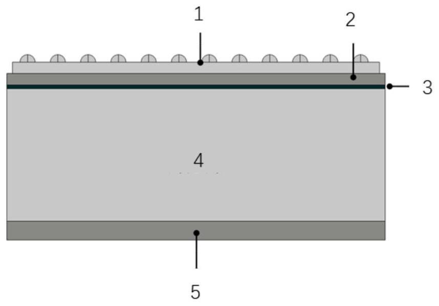
[0048] (1) Use acetone ethanol and deionized water to ultrasonically clean the gallium arsenide substrate epitaxial wafer ((100) crystal plane) (the substrate is 2 inches) in sequence, then take out the substrate and dry it with a nitrogen gun; One side of gallium substrate epitaxial wafer is prepared by evaporation and annealing to prepare gold coating as the back electrode;

[0049] (2) Use wet transfer to transfer graphene to the side of the above-mentioned gallium arsenide that has not prepared the electrode; use vacuum-assisted drying to remove moisture; use gold as the electrode material to vapor-deposit on the graphene surface with a thickness of 100nm, a width of 3 μm, and a spacing of 100nm. A fine grid electrode of 300 μm and a main grid electrode with a thickness of 100 nm and a width of 100 μm distributed along the surface boundary of the graphene layer;

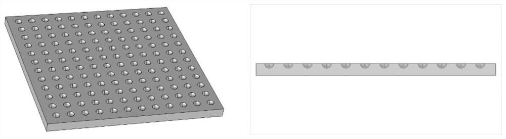
[0050] (3) Add 0.1mL of nano-imprint adhesive (a mixture of GLR Primer tackifier and GLR-Plus UV nano-imprint ...

Embodiment 2

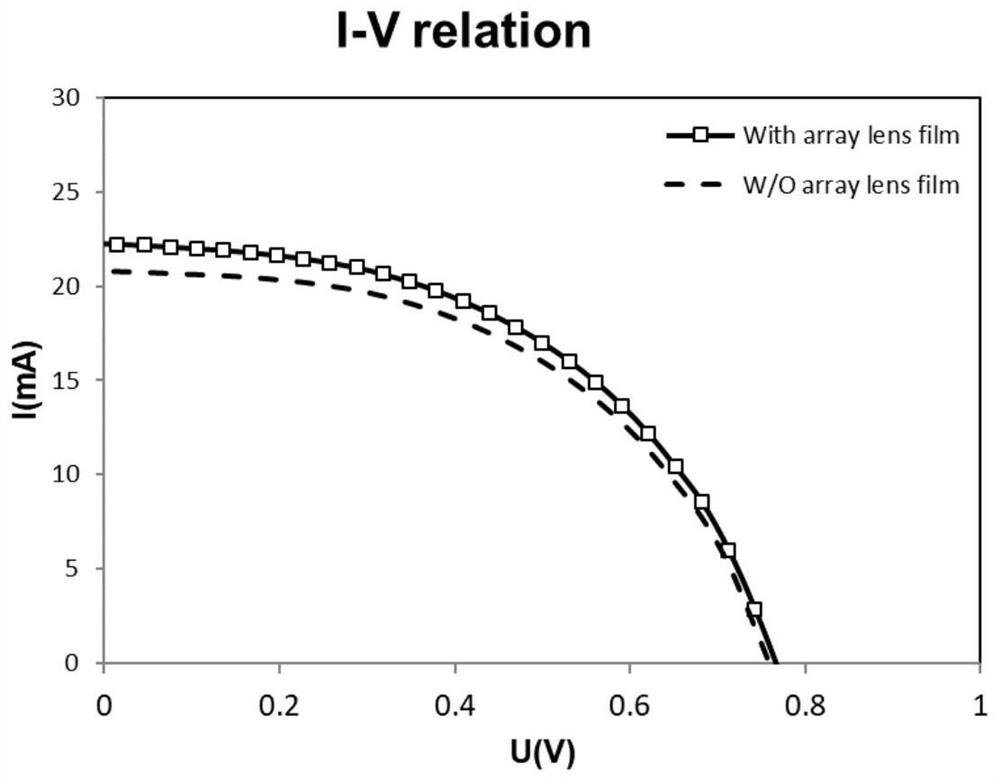
[0057] The difference from Example 1 is that in Example 2, the fine grid pitch of the surface grid electrode is 500 μm, and the thickness of the surface film is changed by controlling the spin-coating time of the embossing glue to 60 s. The pattern parameters of the selected soft film plate are 200nm in diameter, 50nm in thickness, 200nm in pattern array spacing, and 30s of ultraviolet exposure time. Other conditions and preparation methods are the same as in Example 1. The final graphene / gallium arsenide solar cell open circuit voltage V oc is 0.758V, the short-circuit current density I SC 21.3mA cm -2 , the fill factor FF is 50.24%, and the photoelectric conversion efficiency is 8.11%.

Embodiment 3

[0059] The difference from Example 1 is that in Example 3, the spin-coating time of the nanoimprint adhesive is controlled to be 90s, and the pattern parameters of the soft film plate are selected as lens pattern diameter 150nm, thickness 50nm, pattern array spacing 150nm, UV exposure time 90s, other conditions and The preparation method is the same as in Example 1. The final graphene / gallium arsenide solar cell open circuit voltage V oc is 0.758V, the short-circuit current density I SC 22.5mA cm -2 , the fill factor FF is 50.11%, and the photoelectric conversion efficiency is 8.55%.


PUM

PropertyMeasurementUnit
diameteraaaaaaaaaa
thicknessaaaaaaaaaa
thicknessaaaaaaaaaa

Abstract

The invention discloses a graphene/gallium arsenide solar cell with an array micro-nano lens structure and a preparation method of the graphene/gallium arsenide solar cell. The graphene/gallium arsenide solar cell sequentially comprises a back electrode, a gallium arsenide layer, a graphene layer, a gate electrode and a thin film with a surface array micro-nano lens structure from bottom to top. The graphene/gallium arsenide solar cell prepared by the invention has the advantages of higher light utilization efficiency, enhanced light absorption on the surface of the cell, improved photoelectric conversion efficiency and the like, and the prepared thin film with the micro-lens structure can better collect incident light on the surface of the cell, so the photovoltaic effect of the solar cell is facilitated; and the preparation of the graphene/gallium arsenide solar cell with high conversion efficiency is facilitated.

Description

technical field [0001] The invention belongs to the technical field of solar cells, and in particular relates to a graphene / gallium arsenide solar cell with an arrayed micro-nano lens structure and a preparation method thereof. Background technique [0002] In recent years, heterojunction solar cells based on the combination of two-dimensional materials (especially graphene) and semiconductors have attracted great research interest. Although graphene has a very high electron mobility rate, high light transmittance, high thermal conductivity, and excellent photoelectric properties, it is very suitable for use in the photovoltaic field. But its zero bandgap doesn't convert light into electricity efficiently by itself. Therefore, graphene / GaAs heterojunction solar cells based on GaAs semiconductor materials are a good choice for converting incident light into electricity. Current graphene / gallium arsenide heterojunction solar cells have low conversion efficiency. The highest...

Claims


Application Information

Patent Timeline
Patent Type & Authority Applications(China)
IPC IPC(8): H01L31/18H01L31/054H01L31/048H01L31/074B82Y40/00G03F7/00
CPCH01L31/18H01L31/074H01L31/054H01L31/0481G03F7/0002B82Y40/00Y02E10/50Y02E10/52
Inventor 李国强邓曦刘兴江王文樑
Owner SOUTH CHINA UNIV OF TECH
Why Eureka
Try Eureka