Preparation method of angle-insensitive reflective plasma structural color
A plasma and reflective technology, applied in the direction of microstructure technology, microstructure devices, manufacturing microstructure devices, etc., can solve the problems of angle insensitivity, complicated and expensive preparation methods, incident angle sensitivity, etc., and achieve low cost and simple design , The effect of simple preparation process
- Summary
- Abstract
- Description
- Claims
- Application Information
AI Technical Summary
Problems solved by technology
Method used
Image
Examples
preparation example Construction
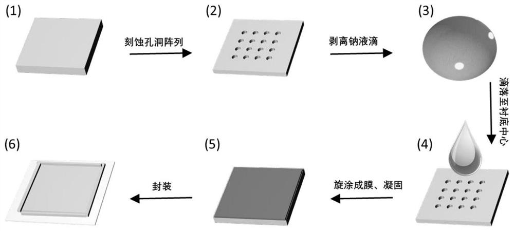
[0033] Such as figure 1 As mentioned, the preparation method of an angle-insensitive reflective plasma structural color according to the present invention, the specific operation steps are as follows:
[0034] (1) Through the FIB (focused ion beam) process, the cylindrical hole array is etched on the quartz plate with the Ag film deposited on the surface;
[0035] (2), soak the quartz sheet etched with the array of cylindrical holes in nitric acid with a concentration of 97.2%, remove the Ag film, clean the quartz sheet with deionized water, and then dry the quartz sheet with a nitrogen gun;
[0036] (3) Place the dried quartz sheet in a muffle furnace, and calcinate it at 600-700°C for 10-30min in an air atmosphere;
[0037] (4), the surface of the hole array of the calcined quartz sheet is etched by an ion beam, and then sent to a glove box equipped with argon as a protective gas to obtain a spin-coated quartz substrate;
[0038] (5) Place the prepared solid sodium block i...
Embodiment 1
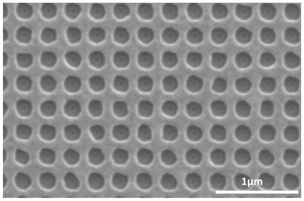
[0052] Hole array quartz plate substrate: Ultrasonic cleaning of the quartz plate substrate with ethanol, after cleaning is completed, it is ready for use; one side of the quartz plate faces the direction of the vacuum evaporation silver target, and by controlling the instrument parameters, 30nm thick silver is evaporated on the surface film; after the evaporation is completed, put the silver film face up and send it to the focused ion beam chamber, set the hole array structure parameters as diameter D=160±20nm, H=70±20nm, P=300±20nm, hole array The area is about 30μm*30μm, and the shape of the hole array on the quartz wafer substrate is shown in the attached figure 2 As shown, it is proved that the hole array structure has good uniformity.
Embodiment 2
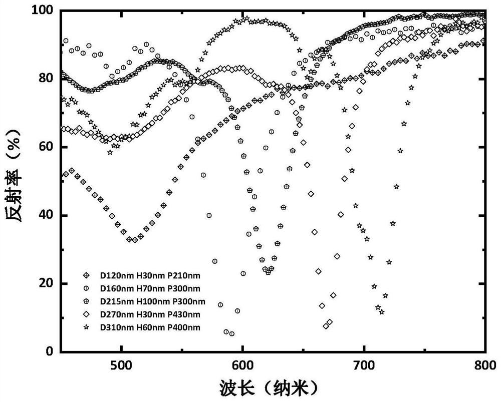
[0054] 1) Preparation of Plasma Structural Color: The preparation method of the hole array quartz wafer substrate in this embodiment is the same as that in Embodiment 1, wherein the structure parameters of the hole array in the step are adjusted respectively D, H, and P, wherein the diameter D is 100-400 nm, and the depth H is 20-100nm, and the period P is 200-500nm; when other conditions remain unchanged, the hole array structure is also obtained on the quartz plate; after the etching is completed, use 97.2% nitric acid to remove the Ag on the surface of the quartz plate, and then use Ultrasonic cleaning of the quartz wafer substrate with ionized water, followed by drying the quartz wafer substrate with nitrogen gas; then placing the obtained quartz wafer in a muffle furnace with the array structure facing up, and calcining at 600-700°C for 10-30min in an air atmosphere After the calcination is completed, the quartz plate array structure surface is evenly etched about 30nm by ...
PUM
 Abstract
Description
Claims
Application Information


