Super junction IGBT device with low loss performance and production method thereof
A low-loss, device-based technology, applied in semiconductor/solid-state device manufacturing, semiconductor devices, electrical components, etc., can solve the problems of weakening conductance modulation effect, large internal resistance of IGBT, weak overvoltage resistance, etc. Effects of extraction, reduced injection efficiency, and high blocking ability
- Summary
- Abstract
- Description
- Claims
- Application Information
AI Technical Summary
Problems solved by technology
Method used
Image
Examples
Embodiment 1
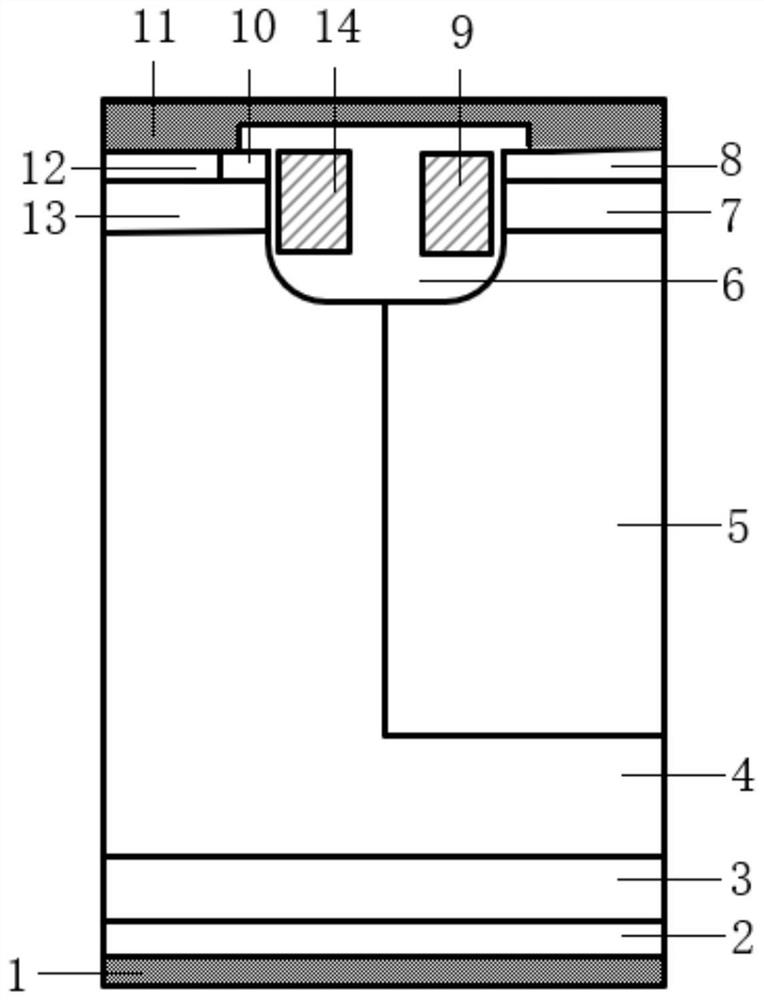
[0018] See figure 1 , figure 1 It is a schematic structural diagram of a super-junction IGBT device with low loss performance provided by an embodiment of the present invention. The device includes: collector (1), P collector region (2), N-buffer region (3), N- pillar region (4), P-pillar region (5), gate oxide layer (6), N-base region (7), P injection region (8), first gate (14), second gate (9 ), N+ implantation region (10), source metal (11), P+ implantation region (12) and P-base region (13).
[0019] The P-collector region (2) is located above the collector (1).
[0020] The N-buffer area (3) is located above the P collector area (2).
[0021] The N-pillar area (4) is located above the N-buffer area (3), and the right side of the N-pillar area (4) is provided with the P-pillar area (5); the P- The horizontal length of the pillar region (5) is half of the horizontal length of the N-pillar region (4).
[0022] The P-base region (13) is positioned above the N-pillar reg...
Embodiment 2
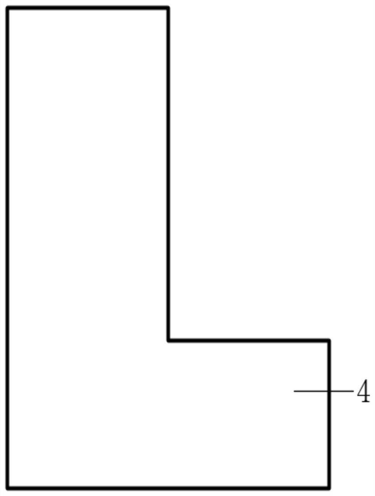
[0053] See Figure 2a-2h , Figure 2a-2h It is a schematic diagram of the manufacturing process of a super-junction IGBT device with low loss performance provided by the embodiment of the present invention. The preparation method of the super junction IGBT device with low loss performance comprises:
[0054] Step 1: The N doping is 3.7×10 15 cm -3 A groove with a depth of 50 μm and a width of 5.5 μm was etched on a silicon wafer.
[0055] see Figure 2a shown.
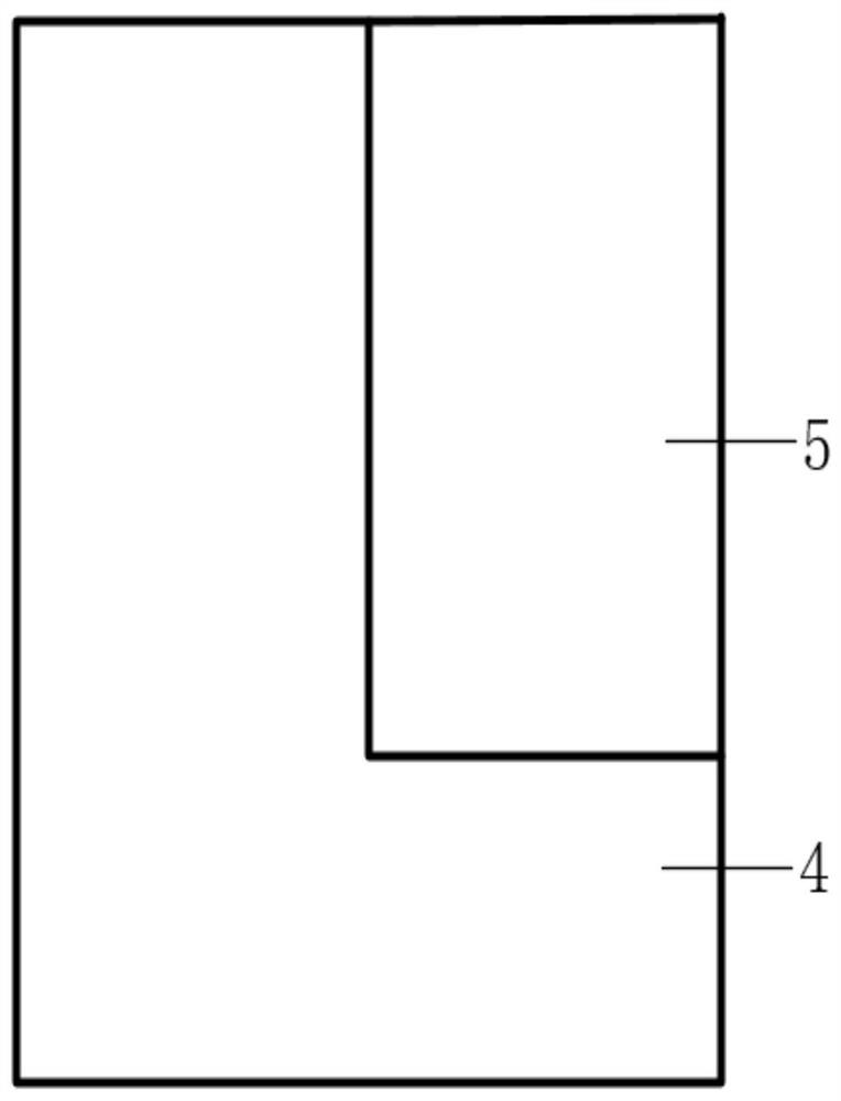
[0056] Step 2: Epitaxially grow P-type silicon in the etched groove as the P-pillar region, doped to 3.7×10 15 cm -3 .
[0057] see Figure 2b shown.
[0058] Step 3: Epitaxially grow a layer of P-type silicon on the silicon wafer with a thickness of 1.7 μm and a doping of 5.1×10 16 cm -3 ; and a layer of P-type silicon is grown on the P-type silicon with a thickness of 0.75 μm and a doping of 8.4×10 18 cm -3 .
[0059] see Figure 2c shown.
[0060] Step 4: Manufacturing a mask and then etching a groo...
PUM
| Property | Measurement | Unit |
|---|---|---|
| length | aaaaa | aaaaa |
| length | aaaaa | aaaaa |
| length | aaaaa | aaaaa |
Abstract
Description
Claims
Application Information


