Semiconductor composite photo-anode, production method and application

A compound light and semiconductor technology, applied in the field of photoelectrochemistry, can solve the problems of high carrier recombination rate and limited photoresponse range of semiconductor materials, so as to improve utilization efficiency, improve photogenerated cathodic protection effect, and improve electron hole transport capacity Effect

Pending Publication Date: 2022-02-08
NORTHWEST NORMAL UNIVERSITY
View PDF5 Cites 1 Cited by
  • Summary
  • Abstract
  • Description
  • Claims
  • Application Information

AI Technical Summary

Problems solved by technology

[0005] The present invention provides a binary semiconductor composite photoanode, a self-assembled ternary semiconductor composite photoanode, a preparation method, and an application in photogenerated cathodic protection, aiming to solve the existing single WO in the above-mentioned background technology. 3 Semiconductor materials have limited photoresponse range and high carrier recombination rate, etc.

Method used


Image

  • Semiconductor composite photo-anode, production method and application
  • Semiconductor composite photo-anode, production method and application
  • Semiconductor composite photo-anode, production method and application

Examples


Embodiment 1

[0033] Example 1 Preparation of semiconductor composite photoanode and its performance testing

[0034] 1. Preparation method

[0035] (1) FTO (conductive glass) pretreatment

[0036] Cut the FTO into small pieces with a size of about 1.5×1cm, then put the FTO into a beaker, and ultrasonically clean it with acetone, ethanol, and distilled water for about 15 minutes for later use.

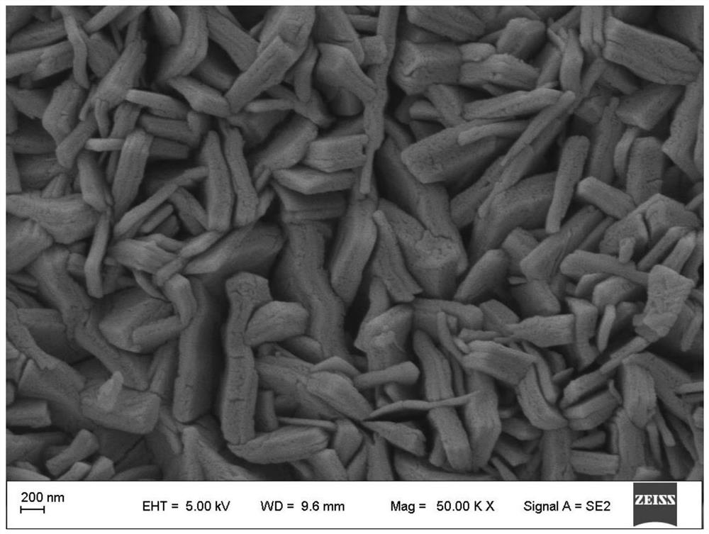
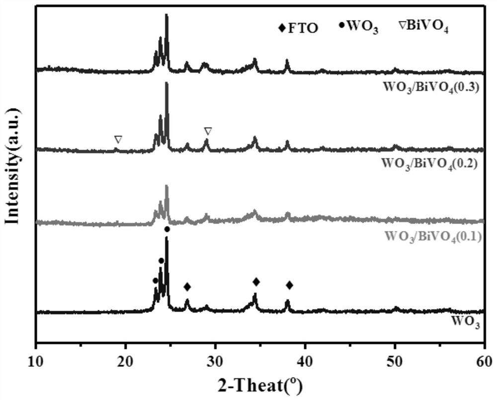
[0037] (2) WO 3 Preparation of the seed layer

[0038] 0.625 g of tungstic acid and 0.25 g of polyethylene glycol-8000 were dissolved in 10 mL of 30 wt % hydrogen peroxide to obtain a yellow solution. Use a pipette gun to drop-coat the solution onto the pretreated FTO, and put it on a homogenizer for spin-coating at a speed of 3000 rpm for 30 s. After the spin coating, the glass sheet was quickly heated in an oven at 100 °C for 10 min, and finally annealed at 500 °C for 2 h in a tube furnace with a heating rate of 3 °C / min, finally forming WO 3 seed layer.

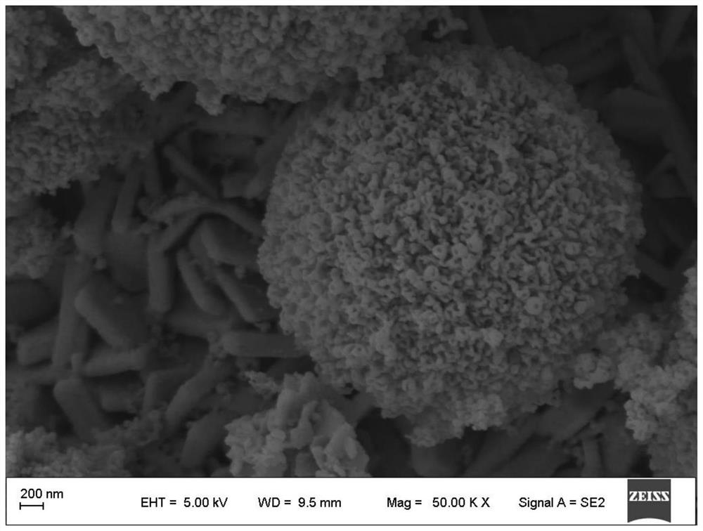
[0039] (3) Preparation of WO-coated...


PUM


Abstract

The invention discloses a binary semiconductor composite photo-anode, a ternary semiconductor composite photo-anode formed by self-assembly, a production method and an application in the aspect of photo-generated cathode protection. The binary semiconductor composite photo-anode is WO3/BiVO4, a WO3 seed layer is prepared on FTO firstly, then a WO3 nano-plate is prepared, then BiVO4 nano-particles are prepared, and the binary semiconductor composite photo-anode WO3/BiVO4 is obtained. Meanwhile, the binary semiconductor composite photo-anode WO3/BiVO4 reacts with Na2S in the electrolyte, Bi2S3 grows in situ, and the ternary semiconductor composite photo-anode WO3/BiVO4/Bi2S3 is obtained through self-assembly. Compared with a pure WO3 sample, the composite photo-anode disclosed by the invention has the advantages that the capturing capability on visible light is enhanced, and the photocurrent density, the electron hole transfer rate and the photoelectric property are improved; and the photo-anode has a more excellent photo-generated cathode protection effect and stability on 304SS.

Description

technical field [0001] The invention belongs to the field of photoelectrochemistry, and specifically relates to a binary semiconductor composite photoanode, a self-assembled ternary semiconductor composite photoanode, a preparation method, and an application in photogenerated cathodic protection. Background technique [0002] As we all know, corrosion has caused a lot of losses all over the world, and the existing anti-corrosion methods consume both energy and materials. Therefore, an energy-saving and environment-friendly anti-corrosion technology is urgently needed. Photogenerated cathodic protection technology is a new type of cathodic protection technology, which is a research hotspot in the field of corrosion protection in recent years. When using photogenerated electrons for cathodic protection of protected metals, one is to select semiconductor materials that can be excited by light to generate photoelectrons; The requirement to transfer and cathodically polarize the...

Claims


Application Information

Patent Timeline
Patent Type & Authority Applications(China)
IPC IPC(8): C23F13/12C23C18/12
CPCC23F13/12C23C18/1216C23C18/1225
Inventor 郭惠霞张玉蓉王珊李亮亮王晓童
Owner NORTHWEST NORMAL UNIVERSITY
Why Eureka
Try Eureka