Silicon carbide single crystal growth device and method

A silicon carbide single crystal and growth device technology, applied in the direction of single crystal growth, single crystal growth, crystal growth, etc., can solve the problems of large resistance, inability to handle mass transmission, insufficient evaporation, etc.

Pending Publication Date: 2022-02-18
宁波合盛新材料有限公司
View PDF7 Cites 7 Cited by
  • Summary
  • Abstract
  • Description
  • Claims
  • Application Information

AI Technical Summary

Problems solved by technology

[0015] In the prior art, the Chinese patent with the publication number CN204570093U discloses a silicon carbide single crystal growth chamber without wrappings. A graphite filter is set between the silicon carbide raw material and the seed crystal on the inner wall of the growth chamber, and the upper surface and the lower surface of the filter are The surface is coated with a high-temperature-resistant metal compound coating, which can filter tiny carbon particles in the decomposition and sublimation stages of raw materials, but cannot handle the tiny carbon particles in the mass transfer stage, and the pore size of the graphite filter is less than 10 microns, which is difficult for this filter processing, and this filter is for Si m C n Atmosphere (with gas phase component Si m C n The gaseous product of unified expression formula (1-1)-formula (1-7), when m=1, n=0, is exactly gaseous Si; When m=n=1, is exactly gaseous SiC; When m=2, When n=1, it is gaseous Si 2 C; when m=1, n=2, it is gaseous SiC 2 ; m C n Atmosphere" is the same as here) the resistance is large, which will easily lead to insufficient evaporation, which will affect the crystal growth rate

Method used


Image

  • Silicon carbide single crystal growth device and method
  • Silicon carbide single crystal growth device and method

Examples


Embodiment Construction

[0036] The following will clearly and completely describe the technical solutions in the embodiments of the present invention with reference to the accompanying drawings in the embodiments of the present invention. Obviously, the described embodiments are only some, not all, embodiments of the present invention. Based on the embodiments of the present invention, all other embodiments obtained by persons of ordinary skill in the art without making creative efforts belong to the protection scope of the present invention.

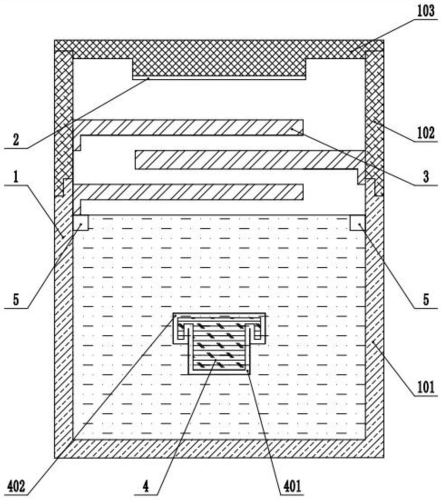
[0037] The purpose of the present invention is to provide a silicon carbide single crystal growth device and method to solve the above-mentioned problems in the prior art, reduce inclusions formed by tiny carbon particles, and prevent inclusions from affecting the quality and crystal growth rate of silicon carbide single crystals.

[0038] In order to make the above objects, features and advantages of the present invention more comprehensible, the present inven...


PUM


Abstract

The invention discloses a silicon carbide single crystal growth device, which comprises a first graphite crucible capable of accommodating silicon carbide powder. At least two layers of graphite baffle plates are also arranged in the first graphite crucible, and the graphite baffle plates divide a channel between silicon carbide seed crystals and the silicon carbide powder into a plurality of communicating channels connected by S-shaped channels. When the silicon carbide single crystal growth device works and the SimCn atmosphere containing tiny carbon particles flows in the communication channel, the tiny carbon particles are subjected to resistance larger than that of gas at the turnings of the communicating channels, and the tiny carbon particles are deposited at the turnings, so that the purpose of reducing wrappage in the silicon carbide single crystal is achieved, and the inclusion is prevented from influencing the silicon carbide single crystal quality and the crystal growth speed. The invention further provides a silicon carbide single crystal growth method, in which carbon particles can be generated in the decomposition and sublimation stages of the silicon carbide powder, the carbon particles move along the communicating channels and are deposited in the communicating channels, silicon steam reacts with the carbon particles, and the silicon carbide single crystal grows on the surface of the silicon carbide seed crystal.

Description

technical field [0001] The invention relates to the technical field of silicon carbide single crystal materials, in particular to a silicon carbide single crystal growth device and method. Background technique [0002] Silicon carbide single crystal material is the representative of the third generation of wide bandgap semiconductor materials, with properties such as wide bandgap, high thermal conductivity, high electron saturation mobility, high breakdown electric field, etc., and the first generation of semiconductor materials represented by silicon and the Compared with the second-generation semiconductor materials represented by GaAs, it has obvious advantages, and is considered to be an ideal semiconductor material for manufacturing optoelectronic devices, high-frequency high-power devices and high-temperature electronic devices. It is widely used in white light lighting, optical storage, screen display, aerospace, high temperature radiation environment, oil exploration...

Claims


Application Information

Patent Timeline
Patent Type & Authority Applications(China)
IPC IPC(8): C30B23/00C30B29/36
CPCC30B23/00C30B29/36
Inventor 章宣赵新田
Owner 宁波合盛新材料有限公司
Why Eureka
Try Eureka