Method for manufacturing selective texturing heterojunction solar cell

A technology of solar cells and manufacturing methods, applied in the direction of final product manufacturing, chemical instruments and methods, sustainable manufacturing/processing, etc., can solve problems such as high defect state density, open circuit voltage drop, and increase the recombination probability of photogenerated carriers. Achieve the effects of cost reduction, enhanced anti-reflection effect, and reduced production process

Pending Publication Date: 2022-03-11
CECEP SOLAR ENERGY TECH (ZHENJIANG) CO LTD
View PDF0 Cites 0 Cited by
  • Summary
  • Abstract
  • Description
  • Claims
  • Application Information

AI Technical Summary

Problems solved by technology

It can be known from theoretical calculations: the more slender the pyramid, that is, the larger the ratio of height / bottom surface area, the easier the incident light is trapped between the pyramids and absorbed by the battery, and the anti-reflection effect is better; and the more slender the pyramid The sharper the edges and corners at the sharp points, edges, and valleys, this leads to the epitaxial growth of the amorphous silicon passivation film deposited and grown in these places. These epitaxially grown films have a higher defect state density, which greatly increases The recombination probability of photogenerated carriers at the amorphous silicon / crystalline silicon interface, resulting in a significant drop in open circuit voltage
The pyramid texture produced on the surface of the silicon wafer by the existing technology has a single texture microstructure, and there is often a contradiction between the anti-reflection effect of the pyramid texture and the deposition quality of amorphous silicon. The sharper the surface microstructure, the better the anti-reflection effect. Well, the flatter the surface microstructure, the better the deposition quality of amorphous silicon, and the better the passivation, which makes it difficult for the surface structure of existing heterojunction solar cells to balance the anti-reflection effect and passivation quality

Method used


Image

  • Method for manufacturing selective texturing heterojunction solar cell
  • Method for manufacturing selective texturing heterojunction solar cell
  • Method for manufacturing selective texturing heterojunction solar cell

Examples


Embodiment Construction

[0024] The present invention will be further explained below in conjunction with the accompanying drawings and specific embodiments.

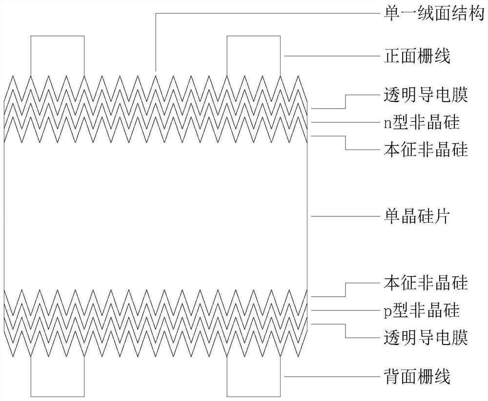
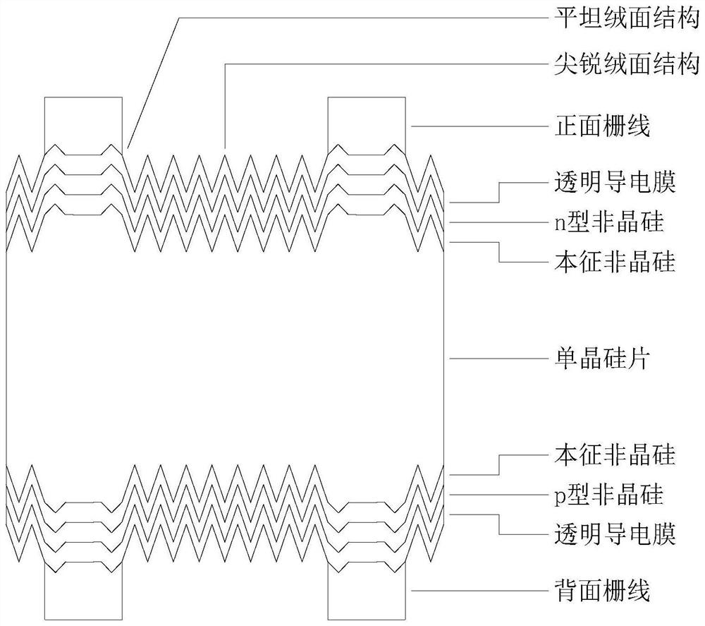
[0025] A method for selectively making textured heterojunction solar cells, combining the attached Figure 8 shown, including the following steps:

[0026] Step 1: Clean the monocrystalline silicon wafer with a cleaning solution at 60-85° C. for 60-300 seconds. The cleaning solution is a mixture of potassium hydroxide, hydrogen peroxide and water at a volume ratio of 1:1:6.

[0027] Step 2: Alkali etching the monocrystalline silicon wafer treated in Step 1 with 60-85° C., 5-25 wt % potassium hydroxide solution for 60-300 seconds, and the etching depth is greater than 5 μm to remove cutting damage.

[0028] Step 3: The single crystal silicon wafer treated in Step 2 is used to make a retardation layer on the required selective texturing area on the surface of the retardation material.

[0029] The selection principle of delaying material: it is...


PUM

PropertyMeasurementUnit
depthaaaaaaaaaa

Abstract

The invention discloses a method for manufacturing a selective texturing heterojunction solar cell, which comprises the following steps of: pre-cleaning a monocrystalline silicon wafer, removing damages, manufacturing a delay layer in a selective texturing area on the surface of the monocrystalline silicon wafer by using a delay material, texturing the monocrystalline silicon wafer, dissolving the delay layer in the selective texturing area by using texturing liquid in the texturing process, and then, preparing a texturing solution in the selective texturing area; and enabling the suede of the selective texturing area to be later than the delay-layer-free area, forming at least two suede microstructures in different position areas on the monocrystalline silicon wafer at one time, and depositing and printing grid lines after texturing to obtain the battery. Different textured microstructures can be formed on the same surface of the same monocrystalline silicon wafer, so that the heterojunction solar cell can obtain the optimal antireflection effect, and meanwhile, the amorphous silicon passivation quality can be greatly enhanced; the delay layer can be arranged differently, different suede microstructures can be formed at a time, the delay material of the delay layer can be directly removed in the texturing process, the production process is reduced, and the cost is reduced.

Description

technical field [0001] The invention relates to a method for manufacturing a heterojunction solar cell, in particular to a method for selectively texturizing a heterojunction solar cell. Background technique [0002] Amorphous silicon / crystalline silicon heterojunction solar cells use [100] oriented monocrystalline silicon wafers, and then use alkaline solution to make texture, so as to obtain a texture with uniform and dense micron-scale pyramids on the surface, which can obtain good anti-reflection effect and increase The incidence of light can effectively increase the short-circuit current of the battery, and then use plasma-enhanced chemical vapor deposition (PECVD) to grow a layer of intrinsic amorphous silicon layer on the surface to passivate the surface, and then the front and back Deposit an n-type amorphous silicon layer and a p-type amorphous silicon layer respectively, and then deposit a transparent conductive film layer on the front and back sides, print grid li...

Claims


Application Information

Patent Timeline
Patent Type & Authority Applications(China)
IPC IPC(8): H01L31/20H01L31/0747H01L31/0236C30B33/10C30B29/06
CPCH01L31/202H01L31/0747H01L31/02366C30B33/10C30B29/06Y02E10/50Y02P70/50
Inventor 李世宇黄惜惜刘海涛张中建王守志高荣刚黄国平
Owner CECEP SOLAR ENERGY TECH (ZHENJIANG) CO LTD
Why Eureka
Try Eureka