Vertical III-nitride power semiconductor device structure with trench isolation layer and preparation method of vertical III-nitride power semiconductor device structure

A technology of power semiconductor and device structure, applied in semiconductor/solid-state device manufacturing, semiconductor devices, electrical components, etc., can solve the problems of unfavorable device forward conduction, large forward conduction resistance, etc., to optimize electric field distribution and improve reverse resistance. voltage capability and the effect of reducing forward on-resistance

Pending Publication Date: 2022-03-22
SHANDONG UNIV
View PDF0 Cites 0 Cited by
  • Summary
  • Abstract
  • Description
  • Claims
  • Application Information

AI Technical Summary

Problems solved by technology

However, in order to form a good depletion region protection, it is required to design the distance between adjacent PN junctions as small as possible, and the small channel width will show a large forward conduction resistance under forward bias conditions, which is not good. Conducive to the forward conduction of the device

Method used


Image

  • Vertical III-nitride power semiconductor device structure with trench isolation layer and preparation method of vertical III-nitride power semiconductor device structure
  • Vertical III-nitride power semiconductor device structure with trench isolation layer and preparation method of vertical III-nitride power semiconductor device structure
  • Vertical III-nitride power semiconductor device structure with trench isolation layer and preparation method of vertical III-nitride power semiconductor device structure

Examples


Embodiment 1

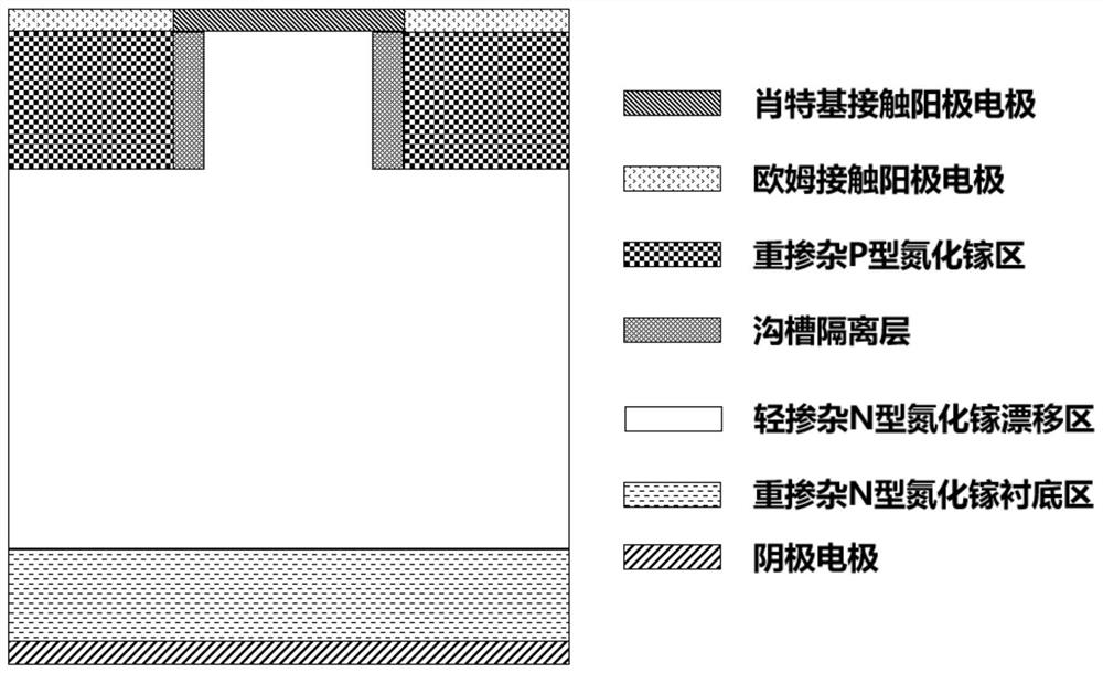
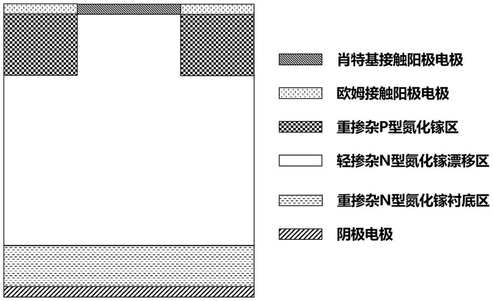
[0055] A vertical type III gallium nitride power semiconductor device structure with a trench isolation layer, the structure is as follows figure 1 As shown, it includes a cathode electrode, a heavily doped N-type GaN substrate region, a lightly doped N-type GaN drift region, a heavily doped P-type GaN region, and an anode electrode from bottom to top; heavily doped An isolation layer of silicon dioxide is arranged between the two vertical contact surfaces of the doped P-type GaN region and the lightly doped N-type GaN drift region, and the lateral thickness of each isolation layer is 50nm. The height is 1.5 μm.

[0056] The doping element of the lightly doped N-type gallium nitride drift region is silicon, and the doping concentration is 2e16cm -3 . The lightly doped N-type GaN drift region is composed of a lightly doped N-type GaN drift layer and a lightly doped N-type GaN protrusion; the lightly doped N-type GaN protrusion has a cuboid structure, The lightly doped N-type...

Embodiment 2

[0063] A method for preparing a vertical Group III GaN power semiconductor device structure with a trench isolation layer described in Embodiment 1, using a secondary epitaxy process to grow a heavily doped P-type GaN region, comprising the following steps:

[0064] (1) Using trimethylgallium (TMGa), ammonia (NH 3 ) as Ga source and N source, SiH 3 CH 3 As an N-type impurity source, H 2 As a carrier gas, a 2μm-thick low-defect, low-dislocation heavily doped N-type gallium nitride substrate region is realized in MOCVD, and the doping concentration of silicon is 5e18cm -3 ;

[0065] (2) Using trimethylgallium (TMGa), ammonia (NH 3 ) as Ga source and N source, SiH 3 CH 3 As an N-type impurity source, H 2 As a carrier gas, a layer of lightly doped N-type GaN drift region with a thickness of 15 μm is homoepitaxially deposited on the surface of the heavily doped N-type GaN substrate region by MOCVD method, and the doping concentration of silicon is 2e16cm -3 ;

[0066] (3) ...

Embodiment 3

[0074] A preparation method of the vertical type III gallium nitride power semiconductor device structure with a trench isolation layer described in embodiment 1, as described in embodiment 2, the difference is: in step (6), use multiple The process of epitaxy plus ion implantation grows heavily doped P-type gallium nitride region, the specific steps are as follows:

[0075] ① Use silicon dioxide as a hard mask to block the top surface of the unetched lightly doped N-type GaN drift region and the upper surface of the isolation layer, use ammonia as the nitrogen source, SiH 3 CH 3 As the dopant source, trimethylgallium (TMGa) was used as the Ga source, H 2 As a carrier gas, a layer of N-type GaN with a thickness of 0.3-0.6 μm is homoepitaxially deposited on both sides of the isolation layer and on the upper surface of the lightly doped N-type GaN drift region by MOCVD method, and the doping concentration of silicon is 2e16cm -3 ;

[0076] ②Use an ion implanter to implant Mg ...


PUM

PropertyMeasurementUnit
thicknessaaaaaaaaaa
thicknessaaaaaaaaaa
thicknessaaaaaaaaaa

Abstract

The invention provides a vertical III-nitride power semiconductor device structure with a trench isolation layer, which sequentially comprises a cathode electrode, a heavily doped N-type nitride substrate region, a lightly doped N-type nitride drift region, a heavily doped P-type nitride region and an anode electrode from bottom to top, and an isolating layer is arranged between the vertical contact surfaces of the heavily doped P-type nitride region and the lightly doped N-type nitride drift region. The arrangement of the trench isolation layer structure optimizes the electric field distribution in the device, effectively improves the reverse performance of the device, and guarantees the excellent forward characteristic.

Description

technical field [0001] The invention relates to a structure of a vertical III-group nitride power semiconductor device with a trench isolation layer and a preparation method thereof, belonging to the technical field of semiconductor devices. Background technique [0002] Compared with the first-generation semiconductors represented by silicon and the second-generation semiconductors represented by gallium arsenide, the third-generation semiconductors represented by silicon carbide and group III nitrides have a large band gap and high critical mass. Excellent characteristics such as breakdown field strength, high thermal conductivity, and high electron saturation drift rate have broad application prospects in high-frequency communication, power electronics and other fields. [0003] At present, the nitride devices that can be widely used are mainly GaN-based lateral high electron mobility transistors (HEMTs). However, the main disadvantage of the lateral device is that the r...

Claims


Application Information

Patent Timeline
Patent Type & Authority Applications(China)
IPC IPC(8): H01L29/872H01L29/06H01L21/329
CPCH01L29/872H01L29/0649H01L29/0619H01L29/66212
Inventor 刘超王珩
Owner SHANDONG UNIV
Why Eureka
Try Eureka