InSb-APD intermediate infrared detector with SACM structure and preparation method of InSb-APD intermediate infrared detector
An infrared detector, N-type technology, used in semiconductor devices, final product manufacturing, sustainable manufacturing/processing, etc., can solve the problems of device dark current increase, high dark current, and narrow band gap material band-to-band tunneling, etc. Achieve the effect of suppressing diffusion current and high gain
- Summary
- Abstract
- Description
- Claims
- Application Information
AI Technical Summary
Problems solved by technology
Method used
Image

Examples
preparation example Construction
[0054] The preparation method of the SACM structure InSb-APD mid-infrared detector of the present invention, the specific steps are as follows:
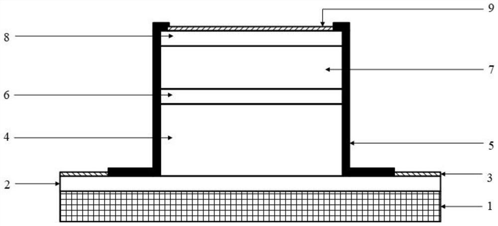
[0055] The N-type InP single wafer was selected as the substrate as the N-type InP substrate 1. After cutting, the substrates were successively prepared on the surface-treated substrates such as ultrasonic cleaning with acetone, anhydrous ethanol and deionized water, and drying at 100 °C in an oven. Floor. The fabrication of the device includes the following steps:
[0056] Step 1, preparation of N-type InP buffer layer 2;
[0057] At room temperature, using InP target, donor dopant. On the N-type InP substrate 1, a magnetron sputtering method is used to deposit an N-type InP buffer layer 2 with a thickness of 0.5 μm at room temperature;
[0058] Step 2, preparation of intrinsic InSb multiplication layer;
[0059] At room temperature, using an InSb target material, a magnetron sputtering method is used to deposit a 3 μm thick uni...
Embodiment
[0076] An N-type InP single wafer was selected as the substrate. After cutting, each layer was prepared sequentially on the substrate after surface treatment such as ultrasonic cleaning with acetone, anhydrous ethanol and deionized water, and drying at 100 °C in an oven. The fabrication of the device includes the following steps:
[0077] Step 1, preparation of N-type InP buffer layer 1;
[0078] At room temperature, an InP target was used, and the dopant was Te. On the N-type InP substrate 1, a magnetron sputtering method is used to deposit an N-type InP buffer layer 2 with a thickness of 0.5 μm at room temperature;
[0079] Step 2, preparation of intrinsic InSb multiplication layer;
[0080] At room temperature, using an InSb target material, a magnetron sputtering method is used to deposit a 3 μm thick unintentionally doped InSb multiplication layer 4 on the basis of the N-type InP buffer layer 2 obtained in step 1;
[0081] Step 3, preparation of P-type InSb charge laye...
PUM
| Property | Measurement | Unit |
|---|---|---|
| Thickness | aaaaa | aaaaa |
| Thickness | aaaaa | aaaaa |
| Thickness | aaaaa | aaaaa |
Abstract
Description
Claims
Application Information
PatSnap Eureka turns technology decisions into work you can execute. Powered by our Innovation Knowledge Graph, it runs expert workflows across engineering, life sciences, materials and intellectual property. Get your review-ready output in minutes.


