Method for preparing negative photoconductive solar blind detector by using beta-phase gallium oxide crystal
A gallium oxide and photoconductive technology, applied in semiconductor devices, circuits, electrical components, etc., can solve problems such as few research opportunities, controversial physical mechanisms, and weak research theoretical foundations, and achieve fast response, high negative response, and performance excellent effect
- Summary
- Abstract
- Description
- Claims
- Application Information
AI Technical Summary
Problems solved by technology
Method used
Image
Examples
Embodiment 1
[0060] A method for preparing a negative photoconductive solar-blind detector using beta-phase gallium oxide crystals, comprising the following steps:
[0061] (1) Preparation of n-type doped gallium oxide substrate: n-type doped Ga oxide by mechanical lift-off 2 O 3 Atomic-level flat and clean surface is obtained, and a gallium oxide wafer is obtained by peeling off mechanically; the electron doping concentration of the gallium oxide wafer is 1×10 18 -5×10 19 cm -3 ; The length of the gallium oxide wafer is 2-4cm, the width is 1-2cm, and the thickness is 10-150μm; the material of the n-type doped gallium oxide substrate is Si-doped gallium oxide;
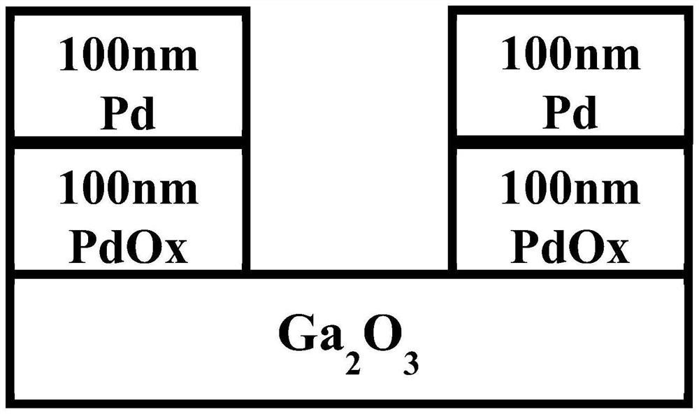
[0062] (2) preparing the negative photoconductive solar-blind detector by successively preparing the gallium oxide wafer obtained in the cleaning step (1), defining the electrode pattern by photolithography, and growing the electrode;
[0063] The definition of electrode patterns by photolithography refers to: preparing electro...
Embodiment 2
[0083] A method for preparing a negative photoconductive solar-blind detector using beta-phase gallium oxide crystal according to Embodiment 1, the difference is:
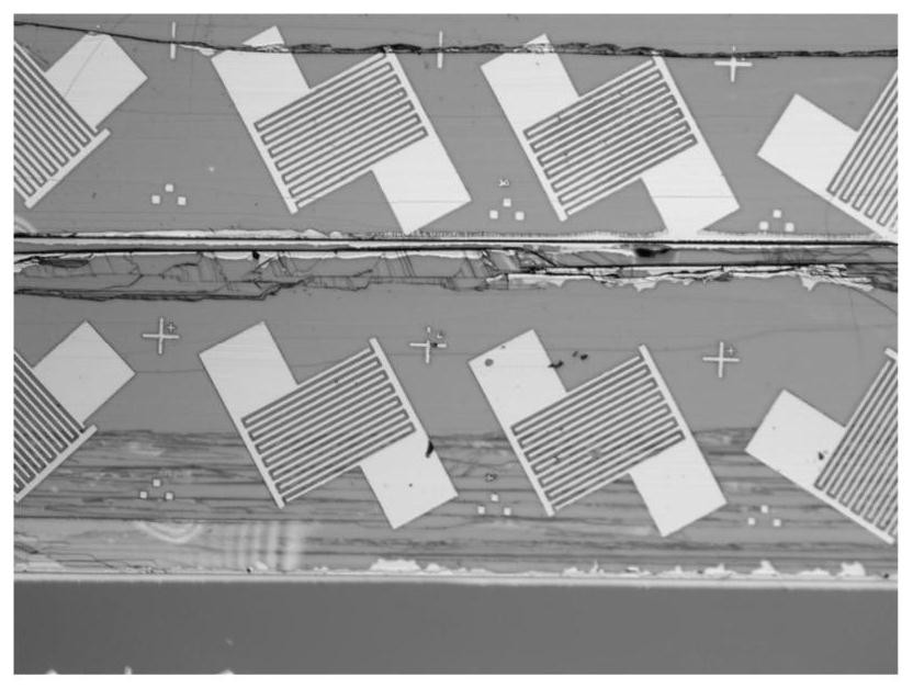
[0084] The electron doping concentration of the gallium oxide wafer is 1×10 18 cm -3 . The gallium oxide wafer had a length of 4 cm, a width of 2 mm, and a thickness of 100 μm. An interdigitated electrode pattern was prepared on the obtained gallium oxide wafer.
[0085] The gallium oxide wafer obtained in the cleaning step (1) refers to: ultrasonic cleaning with 40W power using Dikon cleaning agent for 5 minutes, deionized water 40W power ultrasonic cleaning for 10 minutes, acetone 40W power ultrasonic cleaning for 5 minutes, ethanol 40W power ultrasonic cleaning for 5 minutes, nitrogen gas Reserve after drying.
[0086] Deposition of PdO on Gallium Oxide Wafers X , the process parameters in magnetron sputtering are as follows:
[0087] The sputtering power is 40W;
[0088] The working air pressure is 3.46m...
PUM
| Property | Measurement | Unit |
|---|---|---|
| thickness | aaaaa | aaaaa |
| width | aaaaa | aaaaa |
| thickness | aaaaa | aaaaa |
Abstract
Description
Claims
Application Information


