Optical detection field effect transistor containing quantum point and manufacturing method

A field-effect transistor and light detection technology, which is applied in the direction of semiconductor devices, final product manufacturing, sustainable manufacturing/processing, etc., can solve the problem of increasing the difficulty and complexity of optical-electrical integrated circuit manufacturing, difficulty in controlling the processing and preparation of coupling waveguide layers, The integration of optoelectronic integrated circuits is difficult and other problems, and achieve the effect of simple structure, small crosstalk and high device response efficiency

Inactive Publication Date: 2006-09-13
INST OF SEMICONDUCTORS - CHINESE ACAD OF SCI
View PDF0 Cites 26 Cited by
  • Summary
  • Abstract
  • Description
  • Claims
  • Application Information

AI Technical Summary

Problems solved by technology

Due to the different manufacturing processes of photodetector structures (such as PIN tubes, avalanche photodiodes, APDs, etc.) manufacturing difficulty and complexity
Moreover, the processing and preparation of the coupling waveguide layer is not easy to control
In addition, due to the inherent noise sources (such as dark current noise, quantum noise, etc.)

Method used


Image

  • Optical detection field effect transistor containing quantum point and manufacturing method
  • Optical detection field effect transistor containing quantum point and manufacturing method
  • Optical detection field effect transistor containing quantum point and manufacturing method

Examples


Embodiment Construction

[0035] Below in conjunction with accompanying drawing and specific embodiment the present invention is described in further detail:

[0036] 1. Sample material growth:

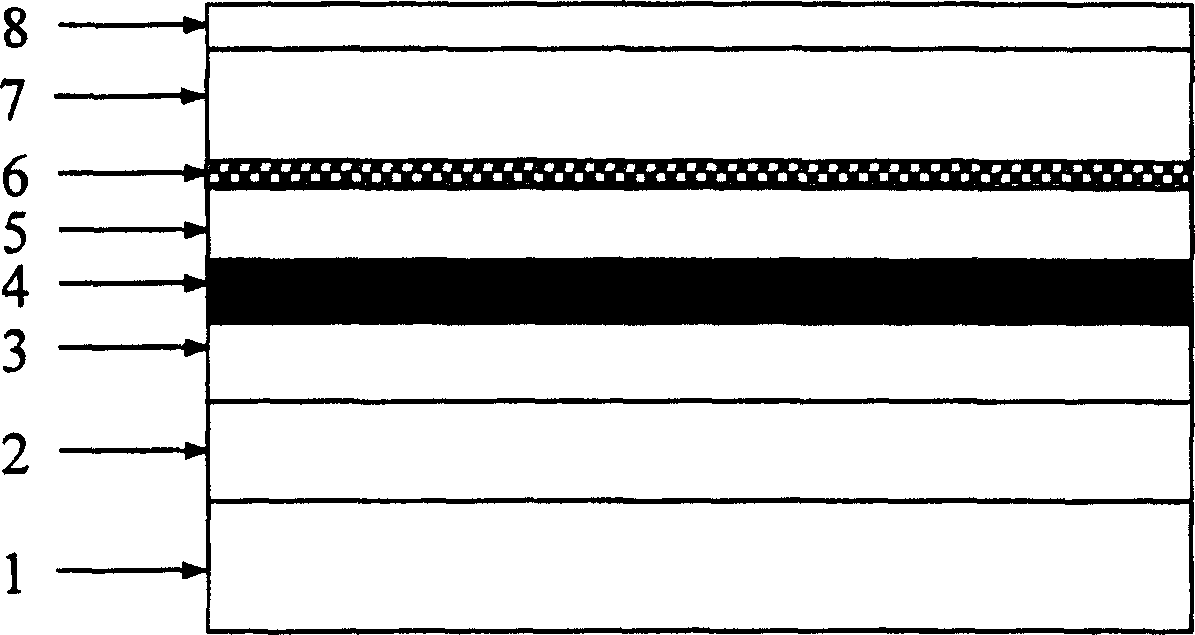
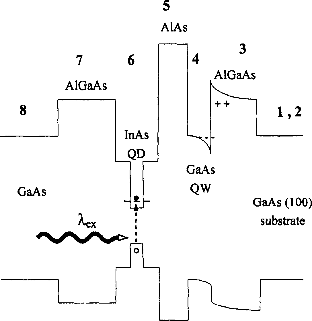
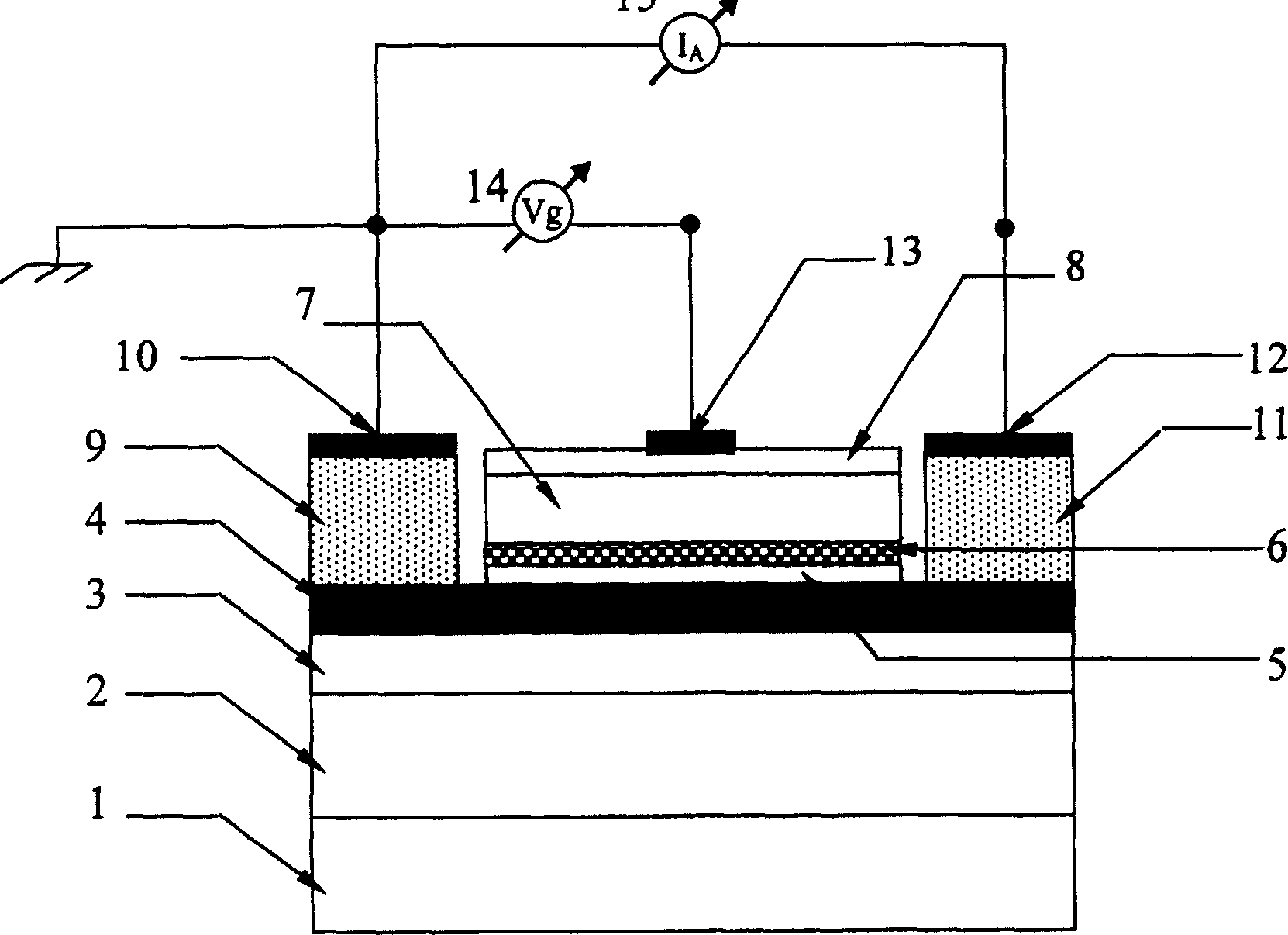
[0037] The device material of the present invention is grown on solid source molecular beam epitaxy (MBE) equipment. figure 1 The device structure shown is that on an N-type gallium arsenide (GaAs) (100) crystalline substrate 1, a gallium arsenide (GaAs) buffer layer 2 is epitaxially grown at a temperature of 600°C; and then a modulated doping structure is grown AlGaAs / GaAs layer, first deposit a 40nm thick doping concentration of 1×10 18 cm -3 (Si) AlGaAs layer 3, followed by growth of 20nm intrinsic gallium arsenide (GaAs) quantum well (QW) channel layer 4. After the growth of the modulation doped layer is completed, 20nm aluminum arsenide (AlAs) is used as the barrier layer 5, and then a layer of self-organized indium arsenide (InAs) quantum dot (QD) layer 6 is grown in the S-K mode at a temperature of 5...


PUM


Abstract

This invention relates to an optical detection field effect transistor containing quantum points and its manufacturing method characterizing: 1, longitudinally integrating a compound semiconductor optical detector and a metal-semiconductor field effect transistor to grow on a same substrate material, 2, separating the active region mesa of InAs quantum points under the grating and the source / drain region to connect the modulated conduction channel under the quantum points with the source / drain to constitute a conducting loop to realize the effective integration of optical devices and electric appliances.

Description

technical field [0001] The invention relates to the technical field of semiconductors, in particular to compound semiconductor field effect transistor devices. Background technique [0002] Semiconductor field-effect transistor (FET) is the basic device unit of modern ultra-large-scale integrated circuit (ULSI), and occupies an extremely important position in the fields of information technology and microelectronics. The basic structure of a field-effect transistor (FET) is a three-electrode device, including a source, a drain, and a gate. The magnitude of the channel current between the source and the drain can be adjusted by changing the voltage applied to the gate, thereby realizing Basic functionality of the device. [0003] Field-effect transistor devices are generally classified into metal-oxide-semiconductor (MOSFET) and metal-semiconductor (MESFET) transistors. Most metal-oxide-semiconductor (MOSFETs) are now made of the elemental semiconductor silicon (Si), becaus...

Claims


Application Information

Patent Timeline
Patent Type & Authority Applications(China)
IPC IPC(8): H01L31/112H01L31/18
CPCY02P70/50
Inventor 曾宇昕杨富华徐萍刘伟
Owner INST OF SEMICONDUCTORS - CHINESE ACAD OF SCI
Why Eureka
Try Eureka