

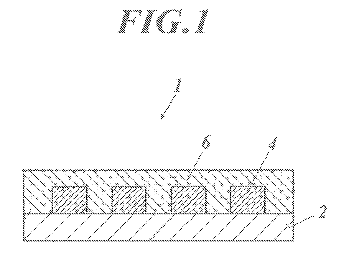
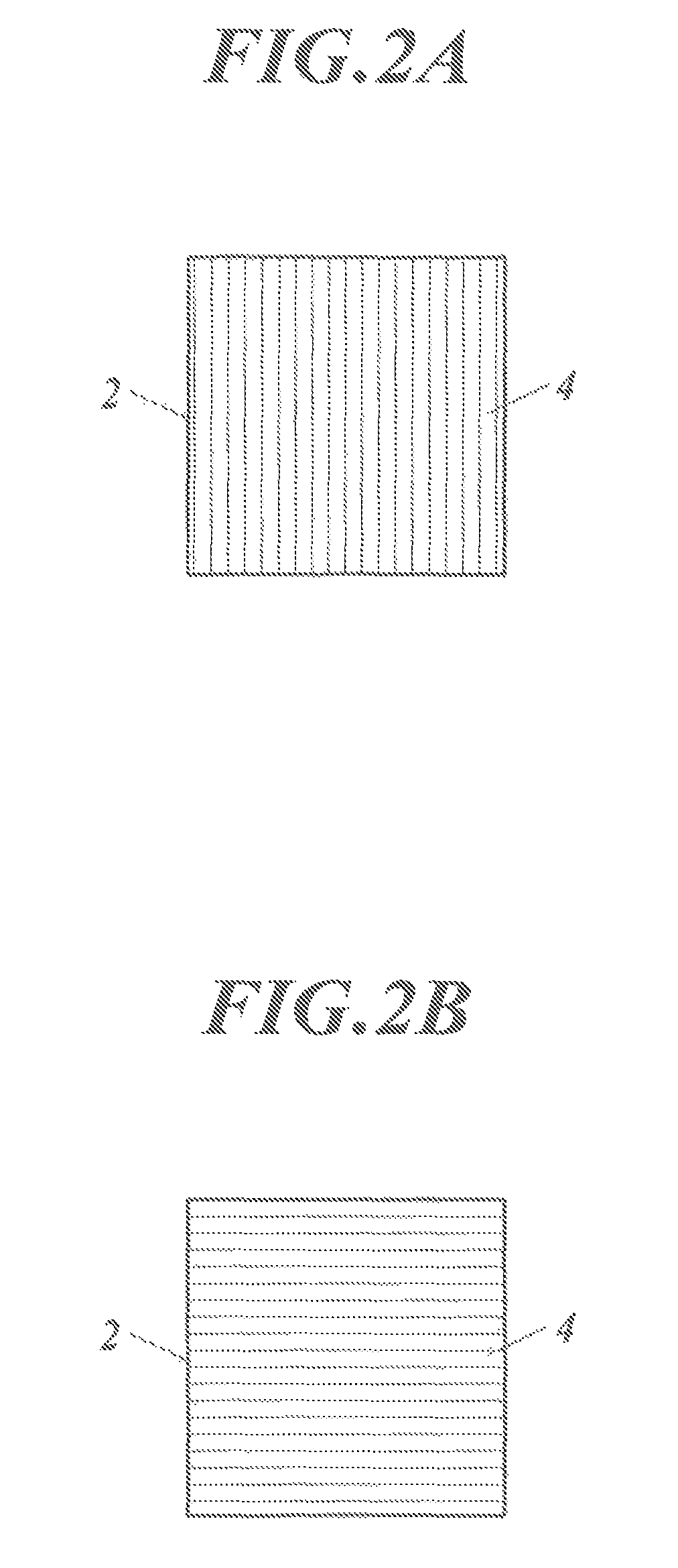
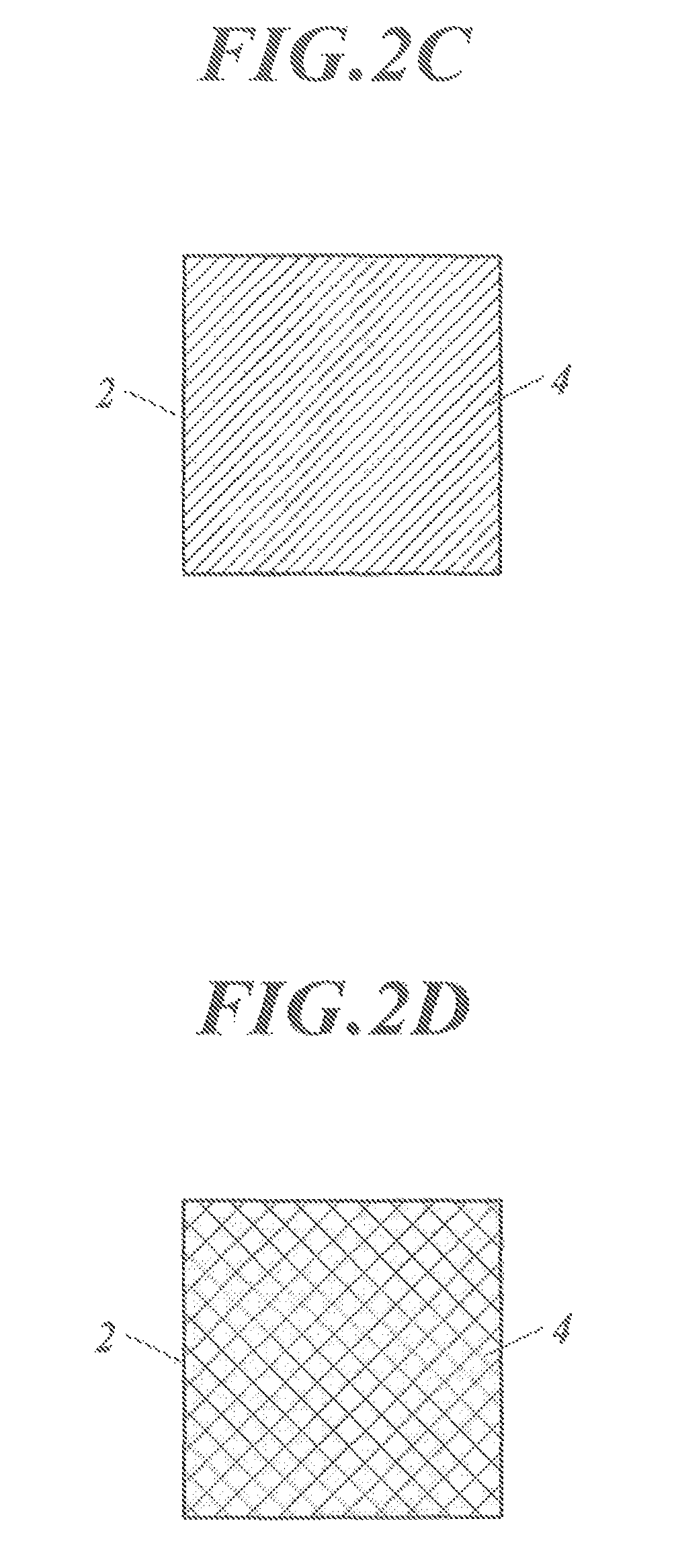
Transparent electrode, organic electronic element, and method for producing transparent electrode
a technology of organic electronic elements and transparent electrodes, applied in the direction of sustainable manufacturing/processing, final product manufacturing, metallic pattern materials, etc., can solve the problems of low productivity, ito-based electrodes which are intrinsically less flexible, and cannot be applied to elements required to be flexible, so as to improve the performance of organic electronic elements and satisfy the transparency and electro-conductivity
- Summary
- Abstract
- Description
- Claims
- Application Information
AI Technical Summary
Benefits of technology
Problems solved by technology
Method used
Image

Examples
example 1
Manufacture of Transparent Electrode (Sample)
(1) Synthesis of Conductive Polymer
[0171]A 2.6% dispersion of poly(3,4-ethylenedioxythiophene) / Nafion (registered trademark) (abbreviated as P-1, hereinafter) was prepared according to a method described in Example 16 of JP4509787B.
(2) Synthesis of Hydroxy Group-Containing Polymer
(2.1) Initiator 1: Synthesis of Methoxy-Capped Oligoethylene Glycol Methacrylate
[0172]In a 50 ml three-necked flask, 2-bromoisobutyryl bromide (7.3 g, 35 mmol), triethylamine (2.48 g, 0.35 mmol) and THF (20 ml) were put, and the internal temperature was kept at 0° C. on an ice bath into the solution, 30 ml of a 33% solution in THF of oligoethylene glycol (10 g, 23 mmol, 7 to 8 ethylene glycol, units, from Laporte Specialties) was dropped. After stirred for 30 minutes, the solution was brought up to room temperature, and further stirred for 4 hours. THF was removed under a reduced pressure using a rotary evaporator and the residue was dissolved into diethyl ether,...
example 2
Manufacture of Organic EL Element (Sample)
[0209]Using the transparent electrodes 201 to 209 manufactured in Example 1, organic EL elements 301 to 309 were respectively manufactured according to the method described below.
(1) Formation of Organic Light Emitting Layer
[0210]On the polymer conductive layer of the transparent electrode, an organic light emitting layer (hole transport layer, light emitting layer, hole blocking layer, electron transport layer) was formed as described below.
[0211]The layers subsequent to the hole transport layer were formed by vacuum evaporation. Predetermined amounts of ingredients, optimized for manufacturing the element were filled in the individual evaporation crucibles of a commercially-available vacuum evaporation apparatus. The evaporation crucibles used herein were those made of materials suitable for resistance heating, such as molybdenum or tungsten.
(1.1) Formation of Hole Transport Layer
[0212]After the apparatus was evacuated to a degree of vacuu...
PUM
| Property | Measurement | Unit |
|---|---|---|
| surface specific resistance | aaaaa | aaaaa |
| surface specific resistance | aaaaa | aaaaa |
| thickness | aaaaa | aaaaa |
Abstract
Description
Claims
Application Information