Method of manufacturing a semiconductor device

a manufacturing method and semiconductor technology, applied in the direction of photomechanical equipment, instruments, originals for photomechanical treatment, etc., can solve the problems of increasing costs, reducing processing accuracy, and requiring many manufacturing processes

Inactive Publication Date: 2002-05-02
HITACHI LTD
View PDF0 Cites 17 Cited by
  • Summary
  • Abstract
  • Description
  • Claims
  • Application Information

AI Technical Summary

Benefits of technology

[0012] It is another object of the present invention to provide a technique capable of shortening a period for developing semiconductor devices.
[0013] It is still another object of the present invention to provide a technique capable of shortening a period for manufacturing semiconductor devices.
[0014] It is yet another object of the present invention to provide a technique capable of decreasing semiconductor device costs.

Problems solved by technology

However, the thus configured mask causes problems of requiring many manufacturing processes, increasing costs, and decreasing the processing accuracy because an opaque pattern is processed with isotropic etching.
First, an opaque pattern comprising the resist layer cannot sufficiently shield the light with a wavelength over 200 nm. Generally, the exposure light such as KrF excimer laser (.lambda.=248 nm) or i-line (.lambda.=365 nm) is used for manufacturing a volume zone on a semiconductor integrated circuit device. An applicable wavelength for the resist layer is critical for the opaque pattern formation.
Second, no sufficient consideration is given about more efficiently manufacturing masks in a short period. In recent years, reflecting a trend of system LSI (Large Scale Integrated) circuits, there is an increasing need for developing and manufacturing a small quantity of, and many types of LSI chip in a short period. The manufacture of these LSI chips uses, for example, 20 to 40 masks. The TAT (turn-around time) for manufacturing masks is a driving force for the LSI development competition. As an advanced feature is requested for this type of LSI chips, the product development requires more processes and a longer period. By contrast, the existing product becomes obsolete soon and the product life is short. It is expected to shorten a period for the product development and manufacture. Especially, a system LSI chip is subject to a high debug ratio for the wire layer. It is important to supply masks for wire layer in a short period and at a low cost for shortening a period and reducing costs for the LSI development. Accordingly, a significant problem is how to efficiently manufacture masks used for this product manufacture in a short time.
Third, no sufficient consideration is given concerning reduction of mask costs. Elements and wires are further fined along with a request to increase integration of elements in a semiconductor integrated circuit device and to increase an operation speed. In addition, strict accuracy is requested for processing mask patterns. An increase in the amount of pattern data remarkably increases mask production costs. Generally, as mentioned above, a plurality of masks is used for one type of semiconductor integrated circuit device. An increase in mask production costs is a serious problem. The technological development progresses with the intention of shortening the exposure light wavelength along with fining of elements and wires. However, shortening the wavelength requires rare and precious lens materials such as CaF.sub.2 and the like. Moreover, optical members are subject to great irradiation damage, shortening the parts life. Hence, the short-wavelength exposure is expensive. When the exposure process for semiconductor integrated circuit devices simply uses a mask having the opaque pattern comprising the above-mentioned resist layer, the ArF excimer laser exposure needs to be used in many cases. Consequently, though the mask cost decreases, the total production cost rather increases.

Method used


Image

  • Method of manufacturing a semiconductor device
  • Method of manufacturing a semiconductor device
  • Method of manufacturing a semiconductor device

Examples


embodiment 1

[0119] (Embodiment 1)

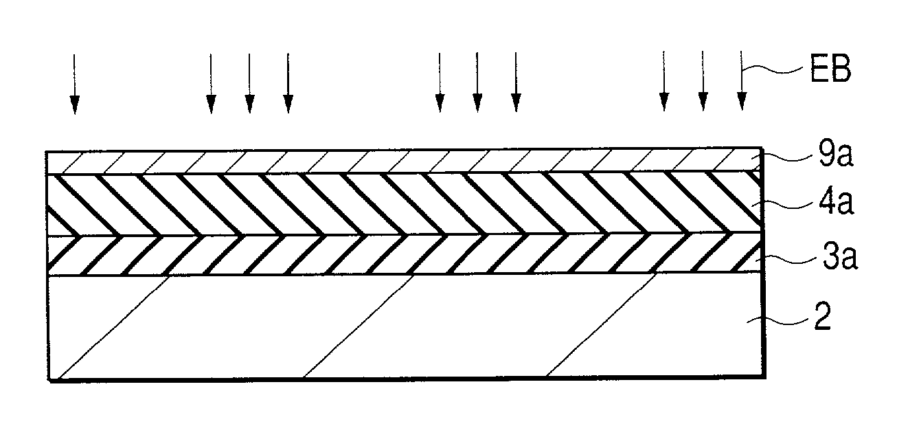
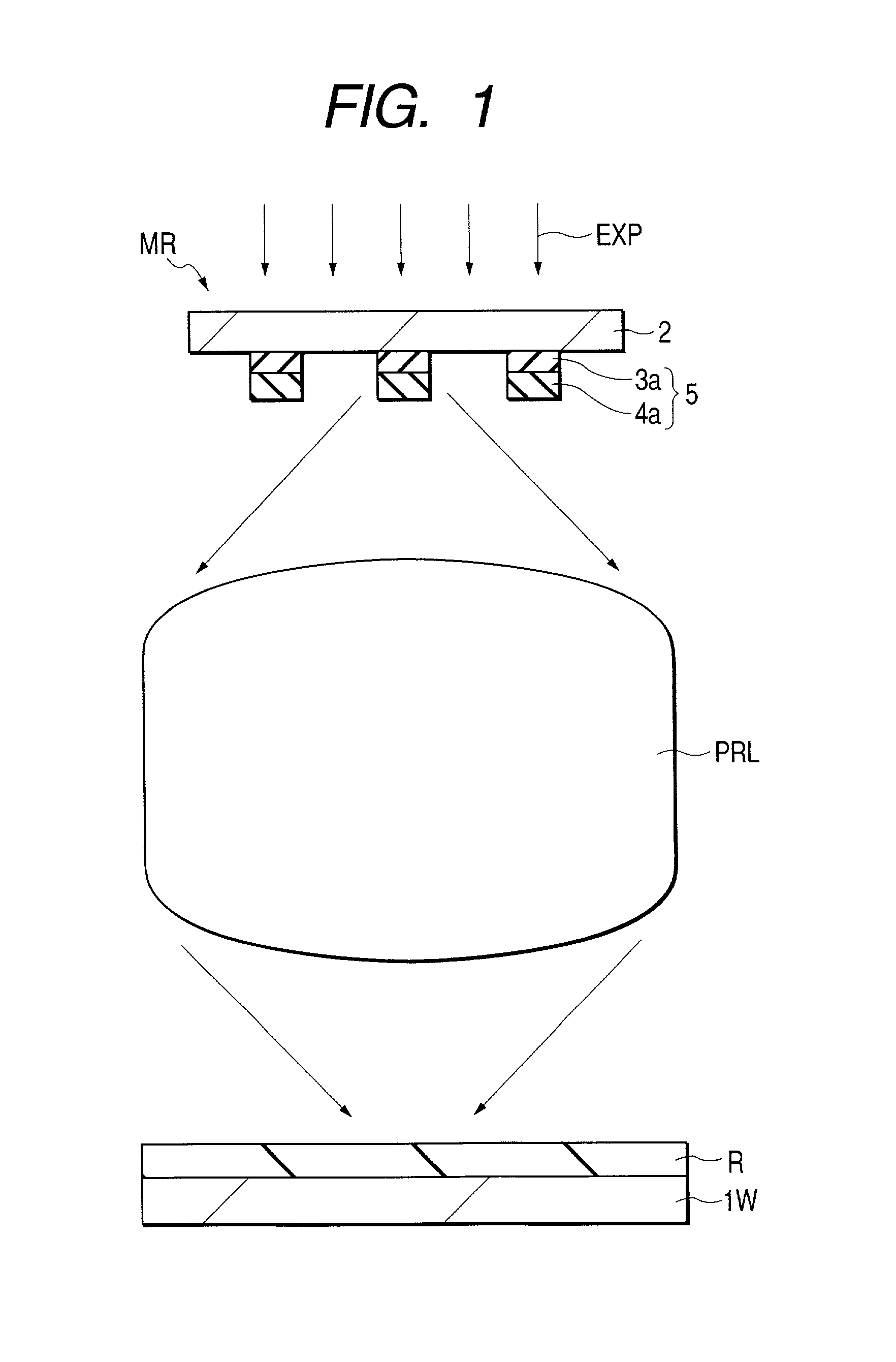
[0120] As shown in FIG. 1 for exposure according to this embodiment of the present invention, exposure light EXP generated from an exposure light source is irradiated onto a mask MR's second principal surface. The exposure light is transmitted through the mask MR. Then, via a projection lens PRL, the exposure light is irradiated to a resist layer R on a wafer 1W mainly comprising silicon single crystal and the like. Here, the above-mentioned ordinary illumination is used. The exposure method may be the scanning exposure or the step-and-repeat exposure as mentioned above. In this embodiment, a plurality of opaque patterns 5 is provided on the first principal surface of a mask plate 2 for the mask MR. Each opaque pattern 5 comprises a layered set of a photoabsorptive organic layer 3a and a resist layer (photosensitive organic layer) 4a. The photoabsorptive organic layer 3a comprises a photoabsorptive or dimming material in reaction to exposure light with a wavelen...

embodiment 2

[0164] (Embodiment 2)

[0165] This embodiment describes how the technological concept of the present invention is applied to the manufacture of mask ROM chips.

[0166] The mask ROM is characterized by providing large-capacity memory because single MIS forms a memory cell and simplifying the entire circuit configuration because no write operation is needed. However, there are problems, too. For example, the mask ROM requires the longer TAT than other ROM chips such as EEPROM (Electric Erasable Programmable Read Only Memory) because memory contents depend on customer requests. Further, different masks must be created according to various customer-based ROM codes, increasing product costs for a small-lot production. In this embodiment, various mask ROM chips with different write data were fabricated as follows. The above-mentioned ordinary mask is used to print a pattern of base data comprising a basic configuration section common to various mask ROM chips. In order to rewrite data, the ab...

embodiment 3

[0175] (Embodiment 3)

[0176] This embodiment 3 is a modification of the above-mentioned embodiment 2. Embodiment 3 explains a case of applying the present invention to a method of manufacturing the mask ROM according to the data rewriting system which differs from the above-mentioned embodiment 2.

[0177] FIG. 29 shows mask ROM base data according to this embodiment. FIG. 29(a) is a layout plan view of the memory cell area. FIG. 29(b) shows its circuit diagram. FIG. 29(c) shows a cross sectional view taken on the line A-A of FIG. 29(a). This example shows mask ROM according to the contact hole program system. The mask ROM according to the contact hole program system performs programming according to a layout of a contact hole (broken lines in FIG. 29(b)) connecting between the semiconductor area 11n and the data line DL. This embodiment also uses the above-mentioned ordinary mask to print the base data pattern.

[0178] Before forming the data line DL with the base data in common, the fol...


PUM

PropertyMeasurementUnit
wavelengthaaaaaaaaaa
exposure wavelengthaaaaaaaaaa
temperatureaaaaaaaaaa

Abstract

Well printing a specified pattern even when exposure treatment using a resist mask uses exposure light with a wavelength over 200 nm. When exposure treatment is applied to a semiconductor wafer 1W by using exposure light EXP with a wavelength over 200 nm, a photomask MR is used. The photomask MR is provided with an opaque pattern 5 comprising a resist layer 4a on a photoabsorptive organic layer 3a in reaction to exposure light EXP.

Description

[0001] 1. Field of the Invention[0002] The present invention relates to a technique for manufacturing a semiconductor device. More specifically, the present invention concerns a technique effectively applicable to the lithography using a photomask (hereafter simply referred to as a mask) during a semiconductor device manufacturing process.[0003] 2. Prior Art[0004] In the semiconductor device manufacturing, the lithography is used as a method of forming a fine pattern on semiconductor wafers. The mainstream lithography is the so-called optical projection exposure method which repeatedly prints a mask-formed pattern on semiconductor wafers via the reduction projection optics. The basic configuration of a stepper is described in, for example, Japanese Patent Application Laid-Open Publication No. 2000-91192.[0005] Generally, resolution R on a semiconductor wafer according to the projection exposure method is expressed as R=k.times..lambda. / NA. In this formula, k is a constant dependent ...

Claims


Application Information

Patent Timeline
Patent Type & Authority Applications(United States)
IPC IPC(8): G03F1/54G03F1/56G03F1/58G03F7/00G03F7/20G03F7/22H01L21/027H01L21/3205H01L21/768
CPCG03F1/56Y10S438/945G03F7/0035G03F1/58G03F1/00H01L21/027
Inventor TANAKA, TOSHIHIKOHASEGAWA, NORIOMORI, KAZUTAKAMIYAZAKI, KOTERASAWA, TSUNEO
Owner HITACHI LTD
Why Eureka
Try Eureka